
.png.7e9d179dfad21bf7eeb93d9dccd1c06a.png)
ultra_code
-
Posts
30 -
Joined
-
Last visited
Content Type
Profiles
Forums
Events
Blogs
Everything posted by ultra_code
-
.thumb.png.be6b3350480379a662a601b9bb3f3631.png) Used InSpectre to disable the Meltdown and Spectre security mitigations within Windows.
Used InSpectre to disable the Meltdown and Spectre security mitigations within Windows. -
Used InSpectre to disable the Meltdown and Spectre security mitigations within Windows.
-
Used InSpectre to disable the Meltdown and Spectre security mitigations within Windows.
-
Used InSpectre to disable the Meltdown and Spectre security mitigations within Windows.
-
Used k10stat to set a single-core ratio on Core 1.
-
CPU has been direct-die cooled. Ran on 3rd core (core #2). Used InSpectre to disable Spectre + Meltdown security mitigations within Windows.
-
Really good chip. :D
-
CPU has been direct-die cooled.
-
Mistake: San Diego is E4, not E3.
-
Mistake: San Diego is E4, not E3.
-
Mistake: San Diego is E4, not E3.
-
Mistake: San Diego is E4, not E3.
-
Mistake: San Diego is E4, not E3.
-
Mistake: San Diego is E4, not E3.
-
Mistake: San Diego is E4, not E3.
-
I like it! XD Thx!
-
Yeah, sure! Of course I've delidded it for testing, so I have both the IHS + CPU photographed, and just the IHS scanned. If you need more photos, let me know.
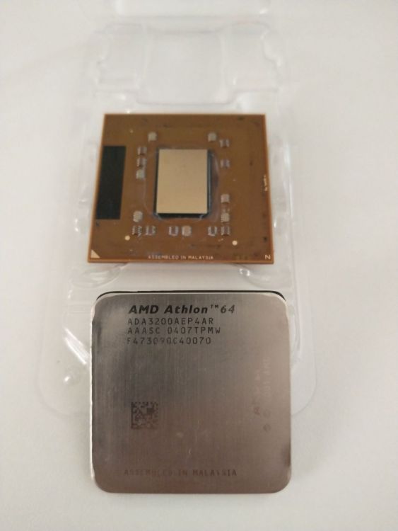
(Clawhammer).thumb.png.7ff3b1b46214fa6226be9de31000cf08.png)
-
Could you please add the Athlon 64 3200+ (2.2Ghz, 512KB) (Clawhammer, S754) to HWBOT? Validation: https://valid.x86.fr/kp9cyh Named the same as the Athlon 64 3200+ (2.0Ghz, 1024KB) (Clawhammer, S754). Strangely, the Athlon 3400+ (Clawhammer, S754) already has two separate categories for it's two SKUs on HWBOT (2.2Ghz, 1024KB; 2.4Ghz, 512KB), but not the 3200+'s.
-
Using I.nfraR.ed's latest X1-1T BIOS.
-
GTL Voltages, Questions Regarding Them
ultra_code replied to ultra_code's topic in General hardware discussion
I've ran into that situation a few times in Cinebench 11.5 (my current default benchmark to run at the moment on S775). Good to know that's what's causing that behavior. Since the original post, I've refined my understand/technique of dealing with VTT (through OCing more quads, of course). I know that CPUs like a certain... range, and it's best to try to maintain it as best as possible. Seems like 45nm quads love VTT (scales with clockspeed, and can save some Vcore in exchange for VTT), whereas the two 65nm quads I've tested are not the least bit interested in any more VTT above the stock 1.2V at around 4Ghz (maybe I'm not at the point where VTT matters for them, maybe they actually need loads of VTT and I've been mistaken, not sure). I suppose my third question in hindsight is a bit silly - why wouldn't you want the lowest VTT you can get away with? Still, if anyone has an edge case where higher VTT for lower ratios is beneficial, let me know. As for the first two questions, I guess I'm asking about something few people know about... :/ -
Hello, First of all, this is my first post on the HWBOT Community Forums. I've been submitting OCing results to HWBOT as a hobby for the past year or so, slowly learning the ropes of different platforms (mainly pre-UEFI-era, e.g. Socket A, 478, and especially 775). Sorry if this forum category is not the best for this post, and please go easy on me if some of these questions should be obvious. Now then, the meat of the matter. As of late, I'm try to get more out of my S775 OCs on water with my Asus P5E3 Premium, and one of things I haven't touched until now are GTL voltages (VTT and the ratios dividing it). Guides on the matter from Edge Of Stability and this Xtreme Systems forum post have helped me wrapped my head around the concept of GTL voltages and such somewhat, but there are still lingering questions I have regarding them. I'm hoping someone here with more experience than me could answers some of my questions. Rather basic question, but where exactly is the GTL circuit(s) located? On the CPU, the northbridge, southbridge, or somewhere else on a motherboard by itself? Are there separate circuits for both the CPU and northbridge, or is it just one circuit handling both? Do they like being cooled, or do they like being ran warm like NAND flash on SSDs? Just for clarity, what are the functions of the "data strobe pins (GTLREF0/2)" and "address strobe pins (GTLREF1/3)"? Also, in the above-linked Xtreme System's forum post, it states that the address strobe pins should be given at a lower voltage/ratio than data pins - could someone vouch for this statement? Any tangible recommendations by how much address strobe pins should be kept below the data strobe pins? Is it better to have lower VTT and higher ratios to compensate, or higher VTT and lower ratios? I'd think the former, but just want some confirmation. If anyone could answer any of these questions, I'd appreciate it. Thanks!
-
Should have been listed under Q9505S, not Q9505 scores.
-
Delidded. Repasted with Thermal Grizzly Kryonaut.
-
Delidded. Repasted with Thermal Grizzly Kryonaut.
-
Delidded. Repasted with Thermal Grizzly Kryonaut.

(Clawhammer).png.9ae36d42c4563fa6423798239a765512.png)