

windwithme
-
Posts
546 -
Joined
-
Days Won
6
Content Type
Profiles
Forums
Events
Blogs
Posts posted by windwithme
-
-
9Cell battery comes with 481g.
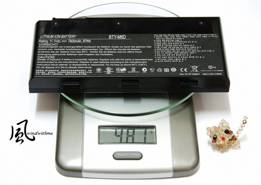
The weight of GT683R is 3436g with battery, lighter than formal number 3.5kg,
if we take a look on the version with single 750GB HDD and 2 DIMM DDR3 4GBx2, it could be lighter around 3.3kg, it’s really not heavy as a gaming laptop.

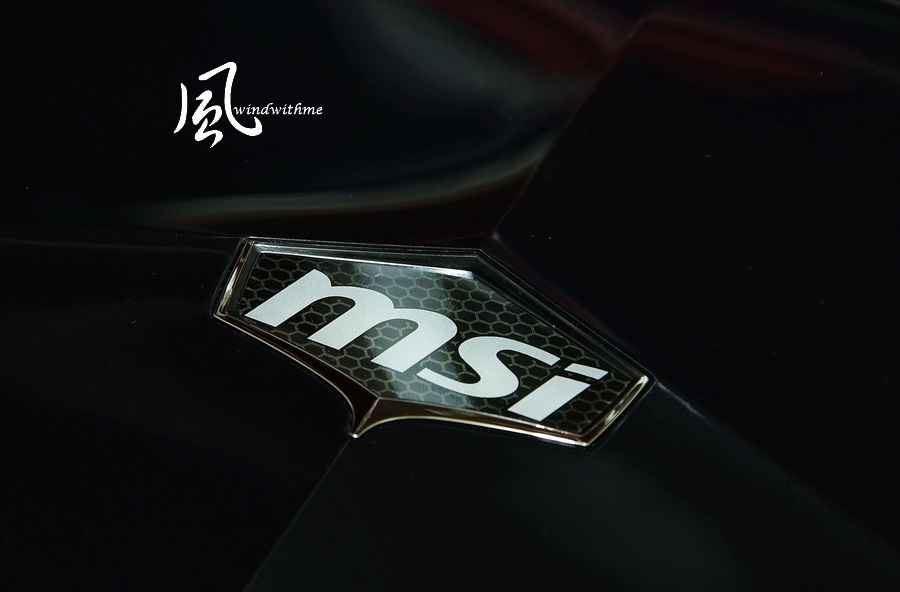
Special designed MSI logo, will show white light when turn on power, it increase the sense of quality.
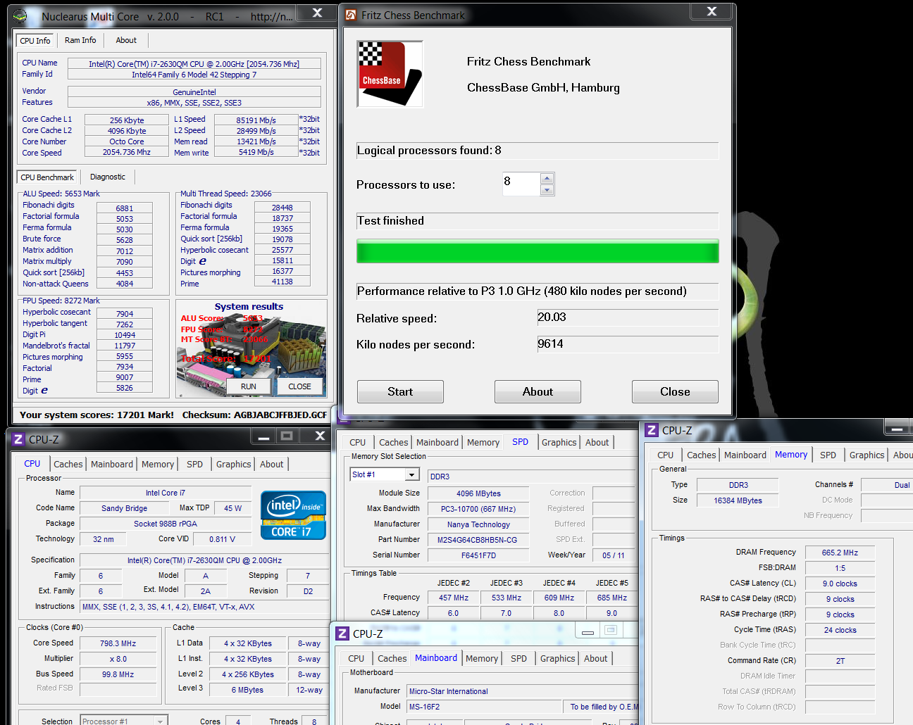
MSI GT683R based on Intel Sandy Bridge platform, use Core i7-2630QM, frequency is 100x20 = 2GHz, L2 = 6MB, 4 Cores with HT technology.
TurboBoost 2.0 technology could increase the frequency up to 2.9GHz, built with HM67 chipset.
Compare with last generation Core i platform, it comes with better performance and newer technologies.
Performance test
Built in with Windows 7 Ultimate 64bit version OS
This version of GT683R is high level version; some region might be selling with lower spec. combination.
HDD is 500GB x2 by RAID 0, 4GB x4 overall 16GB DDR3 and Blu-Ray Combo drive.

Already installed with MSI software, the desk image shows GT683R is great on performance.

System performance tests
Super PI 32M => 22m 31.850s
CPUMARK99 => 439

Nuclearus Multi Core => 17201
Fritz Chess Benchmark => 20.03/9614
CrystalMark 2004R3 => 227107

CINEBENCH 11.5
OpenGL 40.03 fps
CPU 4.82 pts
CPU (Single Core) 1.10 pts
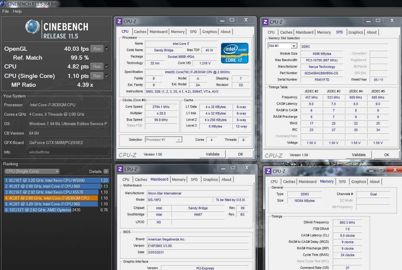
PCMark Vantage => 9297

-
The pad is good on design and touch feeling, very sensitive and easy to handle, 2 keys use brushed looks and feels like metallic, but it’s plastic material.
The light signal on the bottom from left to right is Bluetooth, Wireless, Battery, Sleep mode and HDD.
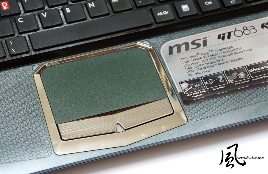
The shield icon in the middle is power button, will show white light when turn on.
Control panel used touch sensor design, with 8 features to turn on and off.
Left 2: Turbo is the GPU overclock function, will enhance 3D gaming performance, for the stability,
MSI will not make overclock range high, but enable Turbo key will unlock the limitation and users could use software to overclock as well.

One of the most important features of gaming is sound effect.
MSI use Sound by Dynaudio 2.1 channel HD speaker system, it present good sound quality as their advantage.

The hinge design is very solid; the open angles almost reach flat 180 degrees.

15.6 inch glossy LED back light panel with 1920x1080 full HD resolutions, MSI adjust on character size to fit this resolution for users.
Built in HD WebCam comes with 30fps 1280x720 video recording and 1280x1024 photo resolution.

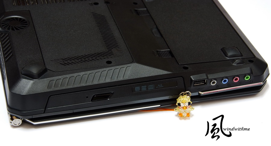
Left side:
Start from left, 1x USB2.0\ multi card reader\ 2x USB 3.0\ heat release holes.

Start from right, Blu-Ray Combo\1x USB2.0\Line out\ Line in\ Mic in\ Headphone out
The back side
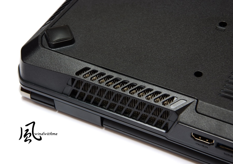
Start from left, 1x HDMI\ 1x eSATA\ 1x D-Sub\ 1x RJ-45 LAN\ AC in

There is another heat release hole in the back, high performance notebooks really take it serious on thermal solution.
The image comes with small subwoofer, this is unusual design, and it really helps on better low frequency sound quality.

-
Notebooks are always a good solution to instead of desktop PCs for most users.
Years ago I always heard my family or friends said that they want to build up new PCs, but in recent years, that voice often become which notebook is better for them to choose.
If users are not demanding on usually upgrade hardware, notebooks always a better solution with higher mobility and better convenience.
The main usage of notebooks comes with 2 types, you might need to analysis your usage before you buy your own laptop.
The first one is business or long time trip, which will need longer battery life and light weight, performance will not be in the high priority.
The second usage is to replace PCs, most because of only have a small room, or long time stay at home or school but need to carry to different places.
This type is more performance oriented demand; users will be more focus on features of higher level CPU, graphics performance, bigger LCD size and high quality speakers.
MSI already building their business for years and now they have 5 different segment of their notebook product lines.
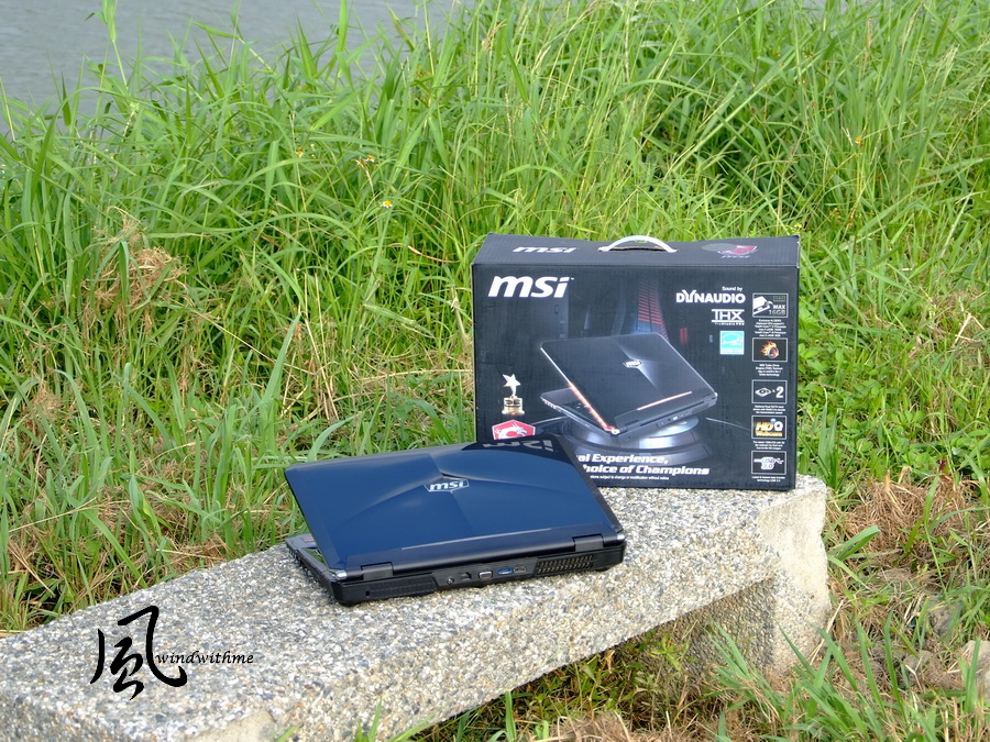
This time I would like to share the 2nd type of notebook, it positioning on Gaming Series, the MSI GT683R.
MSI did have GT680/GT680R in early 2011, so this GT683R should be the upgrade version.

Take a look on the outlooks; GT683R is same as GT680R, built in orange color LED with 7 parts.
The A side cover design is special compare with normal notebooks; it’s more like Alianware and gives a racing car speedy style.
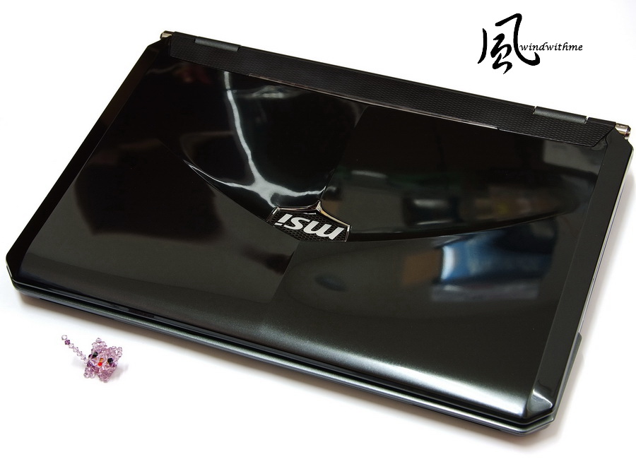
GT683R is black based design, built with latest Sandy Bridge platform with higher performance.
The MSI logo shows white light when boot up, and the silver bar below the logo will show orange color light as well.
The dimension of GT683R is 396mm*265mm*55mm

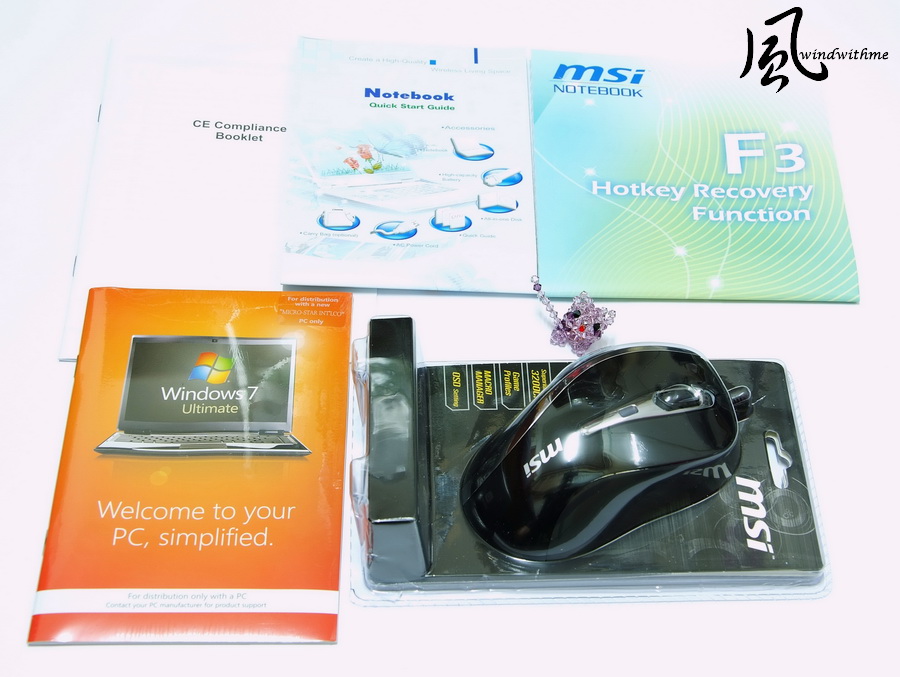
Accessories:
Bundled gaming mouse in GT683R is good to put your hands on and very sensitive feedback.
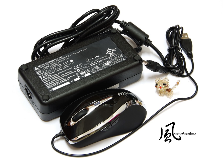
Adaptor is 150W normal version with bigger size, it will show green light when power on, and the temperature is not hot when full loading, hands on will only feel warmer.

The adaptor was made by DELTA, the well known power/ adaptor brand from Taiwan, so the quality is good and reliable, it comes with 4 pads for protection to prevent damage and helpful on reduce
The gaming mouse resolution is 3200DPI, could switch the DPI with the light below the scroll key, also have the page-up/page-down key on the left side, and its light with only 50g weight.
The bottom of the notebook comes with several pad protection, the battery is on down left side, other placement parts are CPU, GPU, HDD, DDR3 and thermal module.
DDR3 comes with 4DIMM design and up to 32GB for users to install, this GT683R comes with 4GBx4 overall 16GB.
Built in with 2 SATA slot supports SATA3 and RAID 0, this is unique for higher storage performance.

Used 9 Cell batteries with 7800mAH, could apply more heavy loading usage for longer time. Remove the battery could see the mechanical detail and Windows sticker.

C side design
The whole cover used the glossy painting with honeycomb surface design and sleek touch feeling.
Regular chiclet keyboard design, use big size placement and independent number keys section, it’s good for most of gaming usages.
The design tone is closer to glossy metallic style, if want to have higher level feeling it might need matted surface treatment with metallic materials.

-
DRAM Bandwidth
DDR3 2278.4 CL10 11-10-27 1T
ADIA64 Memory Read - 10826 MB/s
Sandra Memory Bandwidth - 18915 MB/s
MaXXMEM Memory-Copy - 13200 MB/s
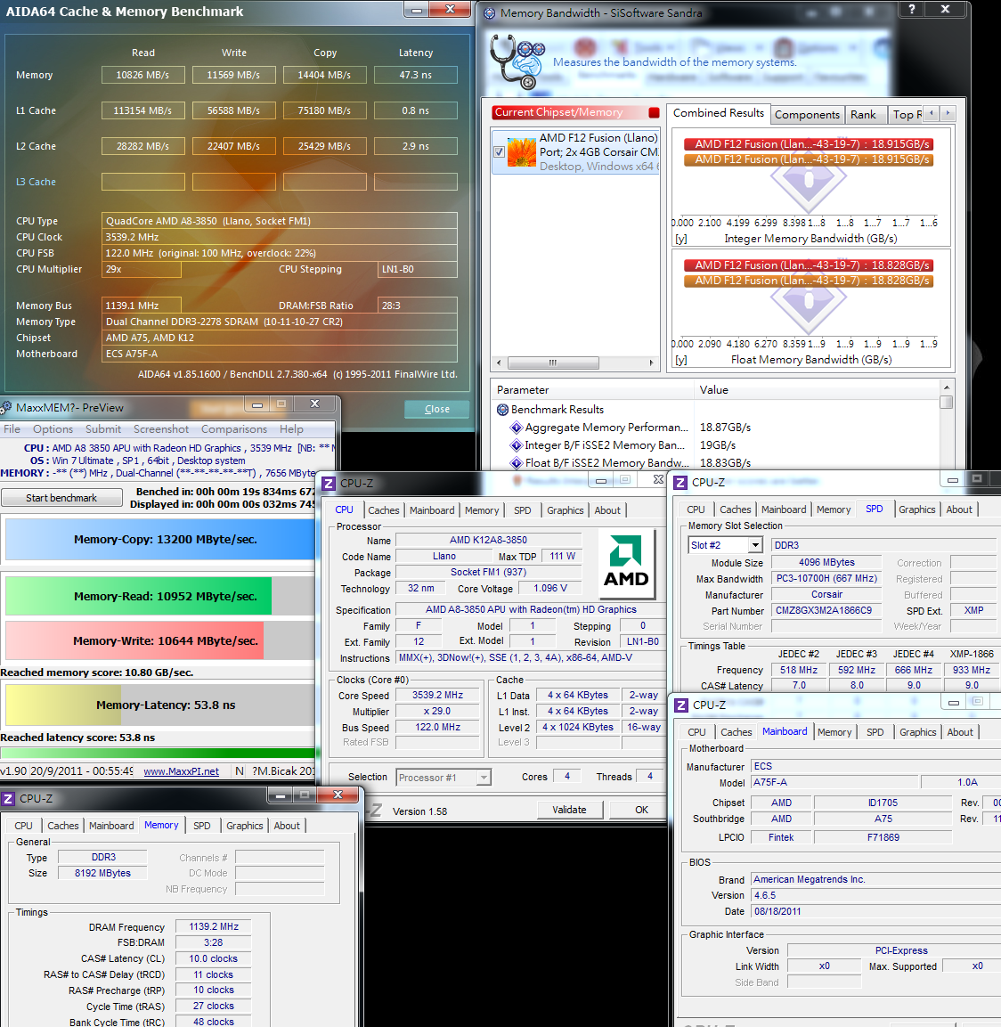
The Llano APU platform has made obvious progress with the DDR3 clock. In the past, the AM3 could only reach the upper limit of about 1800 to 2000 only
This is the first time I’ve seen the AMD DDR3 overclocked to a clock of DDR3 2278, and better compatibility with the physical properties of DDR3 is very important
Bandwidth has increased by about 16 percent, and after the DDR3 clock is pulled up sharply, one of the key areas that AMD needs to improve in the future is bandwidth efficiency
Temperature Performance (room temperature about 26 degrees)
Standby - 5
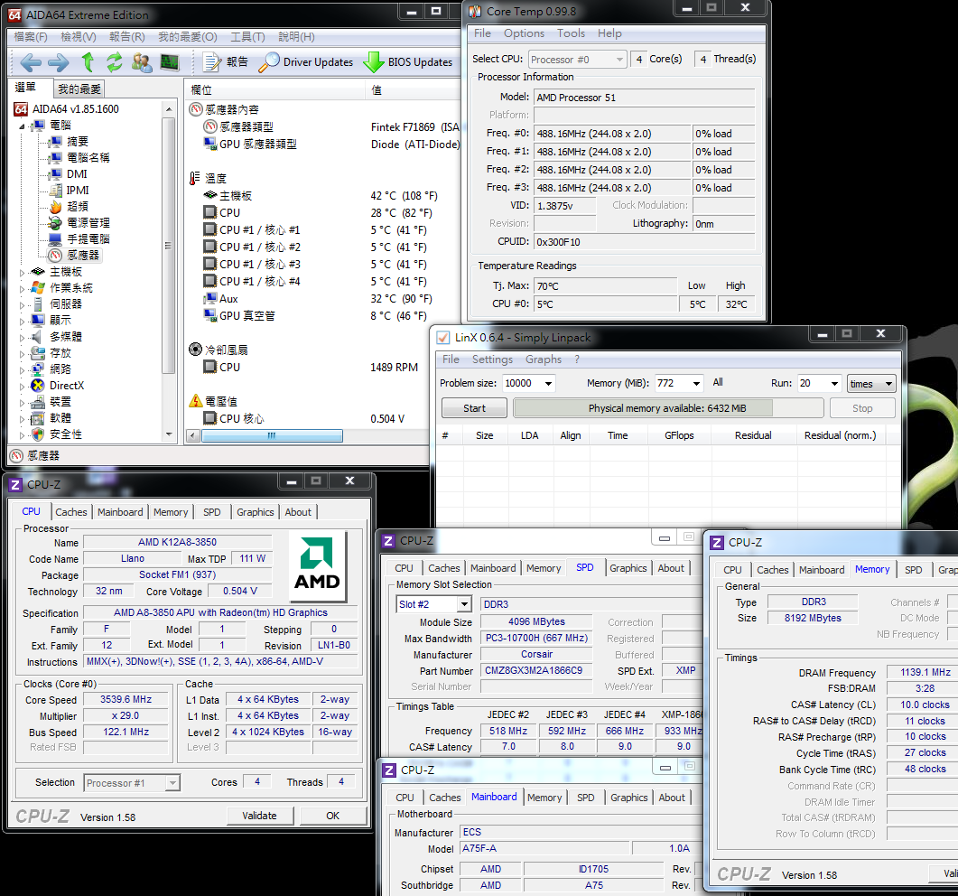
CPU at Full Speed - 50
LinX 0.6.4
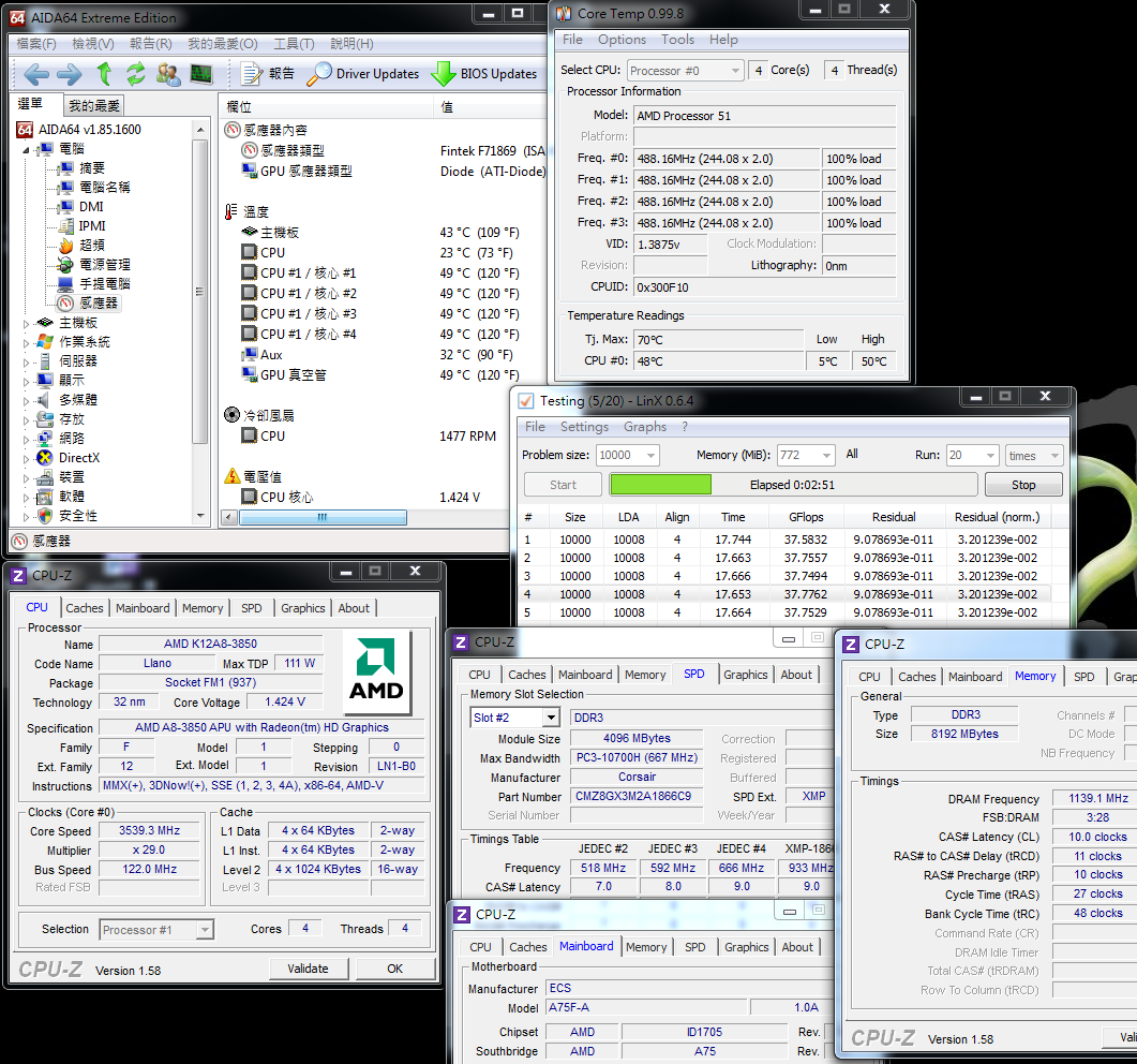
We have tried three A75 motherboard brands, and data showed standby temperatures of 5-18 degrees. This should be a result of C&Q power-saving technology, low voltage and low clock speed.
The temperature of the ECS board at full speed was more than 10 degrees lower than that of the previous A75.
The difference in temperature may be a result of Autumn coming on or the A75F-A temperature monitoring chip
However, the above temperature data shows the 32nm process has reached a necessary level, and temperature performance is fairly good
Power Consumption Test
Standby - 30W

CPU at Full Speed - 167W
LinX 0.6.4

Full speed simultaneously for the CPU and GPU - 210W
Test of the power supply with OCCT
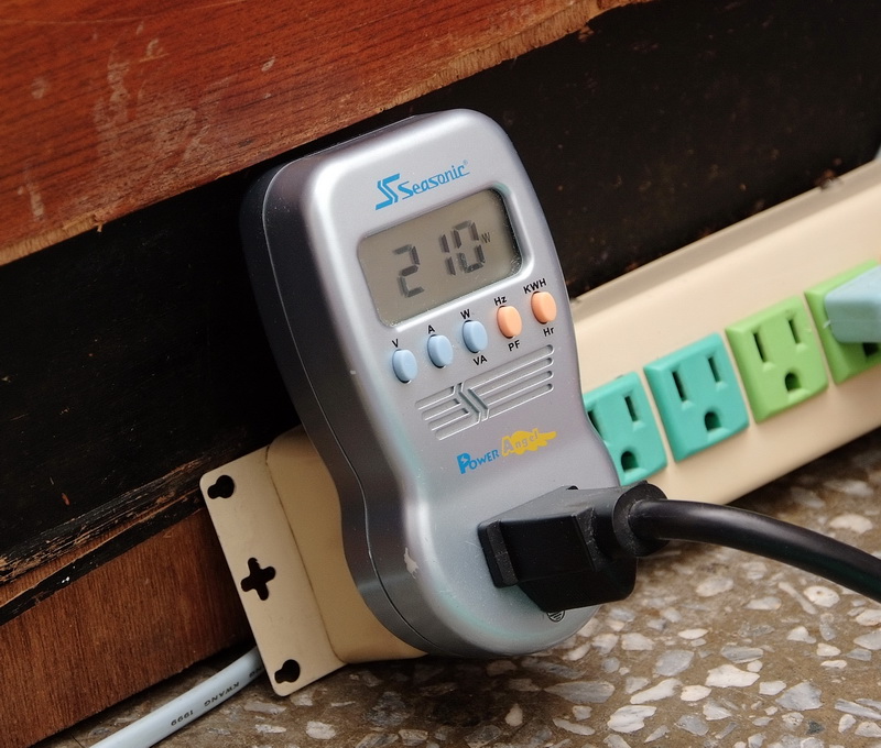
With C & Q power-saving technology enabled and the desktop in standby and when the CPU is operating at full speed, CPU power consumption increases by 137W or so, which is very high data
The GPU increases by about 43W, and at such a high performance level for the GPU, power consumption is still within an acceptable range
Although Llano APU is now fabricated with a 32nm process, the power performance still leaves room for improvement
3D Test
Internal AMD Radeon HD6550D display driver
3DMark Vantage => P5451

StreetFighter IV Benchmark
1920 X 1080 => 70.21 FPS

FINAL FANTASY XIV
1920 X 1080 => 1171

The Llano APU’s internal performance mainly depends on level of the DDR3 clock When overclocking reaches DDR3 2278, there is an approximate 23 - 30% increase in 3D performance.
In high-resolution environments, as long as the 3D game is not too demanding and not too many 3D effects are enabled, the system should be able to operate smoothly
In the past, the gap in performance with entry-level VGA display was often as much as 5 to 10 times.
In this year’s battle, the Llano APU’s 3D performance has attained almost the same level as entry-level VGA.
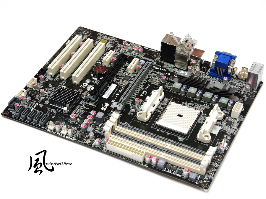
ECS A75F-A
Advantages
1. ECS has moved the BIOS to the UEFI interface, and many optional languages are available
2. CPU and DDR3 overclocking ability is good, helping improve system performance
3. PCI-E/PCI provides a sufficient and convenient number of expansions, and the A75 includes native SATA3 and USB 3.0 technology
4. Three display output interfaces are provided that together with the A8/A6 CPU provide very dazzling 3D performance
5. Heat dissipation is well implemented, and while the power is on heat sink and chipset temperature is not high
Shortcomings
1. The visibility of sales channels and service providers can be further enhanced
2. When the CPU is overclocked to 107MHz or more only the IDE mode can be used. We hope that the BIOS can be revised
Performance ratio ★ ★ ★ ★ ★ ★ ★ ★ ☆ ☆
Material comparison ★ ★ ★ ★ ★ ★ ★ ★ ☆ ☆
Specification comparison ★ ★ ★ ★ ★ ★ ★ ★ ★ ☆
Appearance ★ ★ ★ ★ ★ ★ ★ ☆ ☆ ☆
Cost-effectiveness ★ ★ ★ ★ ★ ★ ★ ★ ★ ☆
When playing a Blu-ray movie, using the previously mentioned 1080P video playback, CPU usage rose as much as 10%
The Intel internal HD2000/3000 GPU is of a comparable standard, and the new generations of the two brands can easily cope with 1080P
The A75’s six internal SATA3 mechanisms are a significant difference compared with the native USB 3.0 technology of the A55
Although the A75 is a bit more expensive than the A55, it still falls within mid-range market price points
If you want a cheaper combination, of course the A55 will save some money, but if you want outstanding specifications, we suggest you consider budgeting a little more for the A75

ECS has currently introduced three A75 motherboards, and this review is only for the A75F-A Black Series product with the ATX specification
The A75F-A has a price of about NT$2900 or less, (equivalent to a retail price of about US$84.99) which is cheaper than some other A75 ATX brands
Combining the UEFI interface, plenty of IO and ample PCI-E/PCI expansion slots as well as excellent overclocking features and more.
The A75F-A’s cost to performance value is quite good, and we hope more value-added products will be introduced for consumers to choose from
This article is windwithme’s third overclocking test of the A75, and each one provides detailed insight on performance, teaching methodology and the overclocking experience
This is provided as detailed reference for consumers who are interested in buying new platforms using the AMD Llano APU. Thanks

This article is also post in my own blog WIND3C Welcome your visit.
-
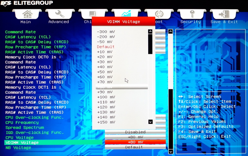
VDIMM Voltage -300~+600 mV
NB Voltage +10~+360 mV
DDR3 Frequency Options
Built-in GPU that can share main memory capacity of 64M - 2GB

Hardware Status
Added Smart Fan speed control function

Details about overclocking have been mentioned previously.
When the Llano APU pulls the CPU to a higher clock, the SATA FSB will be pulled up at the same time
For an extended time under 100MHz non-overclocked conditions, the stability of the SATA device may be uncertain
This occurs with the entire A75/A55 series under overclocking conditions, and this is an inherent physical limitation in AMD’s design
For a wide range of users who want to overclock the CPU, we recommend that you wait for the launch of CPUs that are not locked.
Increasing the multiplier is a better solution for overclocking
With the AMD Llano APU, overclocking settings are a bit simpler
Just pull up the CPU FSB and combine that with the appropriate voltage to achieve overclocking results
Of course, you’ll need to choose the right DRAM to effectively and simultaneously boost DDR3 and GPU performance
Above are the overclocking settings from windwithme for the A75F-A for use as reference
Overclocking Performance Test (SATA to IDE mode)
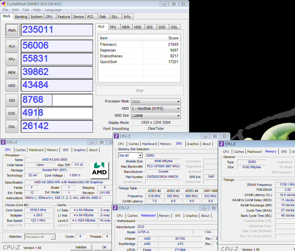
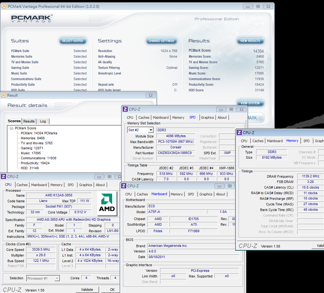
CPU 122.0 X 29 => 3539.4MHz
DDR3 2278.4 CL10 11-10-27 1T
Hyper PI 32M X 4 => 19m 01.017s
CPUMARK 99 => 510

Nuclearus Multi Core => 15036
Fritz Chess Benchmark => 18.07/8671

CrystalMark 2004R3 => 235011
CINEBENCH R11.5
CPU => 4.18 pts
CPU(Single Core) => 1.07 pts

PCMark Vantage => 14304
Windows Experience Index - CPU 7.4

When the A8-3850 overclocked from 2900MHz to 3540MHz, the CPU performance increase was about 20%
Compared with the 32nm process CPU, overclocking added about 1.45V to the required voltage.
This relationship between the clock and voltage did not result in significant progress.
Although the performance of the A8-3850 CPU has been sufficient for most environments, consumers would like to see more progress with the new architecture
-
Power Consumption
Standby - 27W
CPU Full Speed - 125W
LinX 0.6.4

Both the CPU and the GPU simultaneously at full speed - 153W
With OCCT running, a test of the power supply

In standby mode, because of the AMD C&Q power-saving technology, power consumption is reduced to only 27W
With the Llano APU platform, the main power consumer is the CPU. At full speed, there is an increase of about 98W in CPU power consumption
In addition, following our comparisons, we believe that the ECS had more outstanding power performance,
and the A75F-A was about 10-20W lower than the previously used A75 platform
3D Test
Internal AMD Radeon HD6550D display driver
3DMark Vantage => P4423

StreetFighter IV Benchmark
1920 X 1080 => 57.58 FPS

FINAL FANTASY XIV
1920 X 1080 => 947
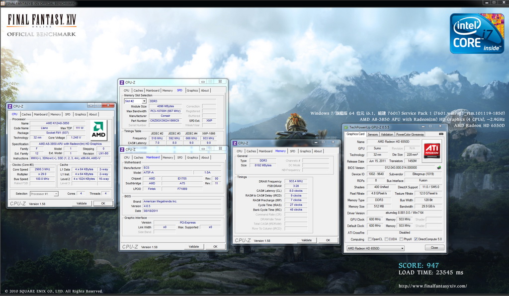
Built-in 3D performance is the biggest advantage of this platform, and the largest factor boosting the performance level is the DDR3 clock
When combined with top of the line DDR3, taking the setting to 1866 will result in a significant 3D performance boost
The above test data showed the internal 3D almost on a par with the nVIDIA GT430, and slightly better than the AMD Radeon HD5570
Consumers who want to buy entry-level VGA should save their budget with this expenditure
ECS brought the BIOS interface to the UEFI, and this new specification is what most of the motherboard brands have pursued in 2011
Main Screen

Quite good support is provided with options for multiple languages

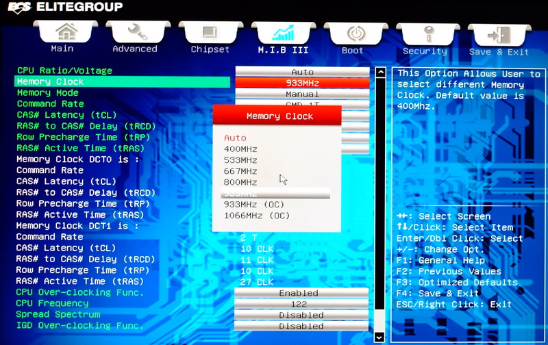
M.I.B III Overclocking Page
At the top are mainly the CPU multiplier, DDR3 clock and parameter settings
In the middle are current parameters for the DRAM
Below are the CPU FSB overclocking settings. This has a very significant impact on the Llano APU

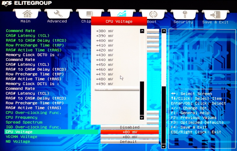
Voltage Range
CPU Voltage +10 - +500 mV
-
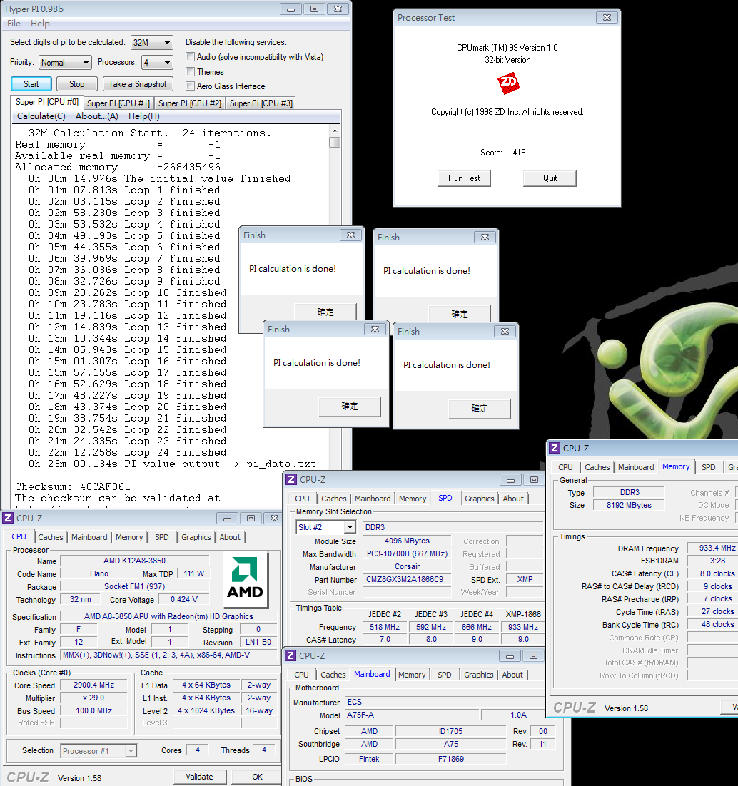
Test Platform
CPU: AMD A8-3850
MB: ECS A75F-A
DRAM: CORSAIR CMZ8GX3M2A1866C9R
VGA: AMD Radeon HD6550D
HD: CORSAIR FORCEGT 120GB
POWER: Thermaltake TR2 450W
Cooler: Thermaltake BigTyp 14Pro
OS: Windows7 Ultimate 64bit SP1

CPU Default Performance Test
CPU 100.0 X 29 => 2900.4MHz
DDR3 1866.8 CL8 9-7-27 1T
Hyper PI 32M X 4 => 23m 00.134s
CPUMARK 99 => 418
Nuclearus Multi Core => 12315
Fritz Chess Benchmark => 14.86/7131

CrystalMark 2004R3 => 200725
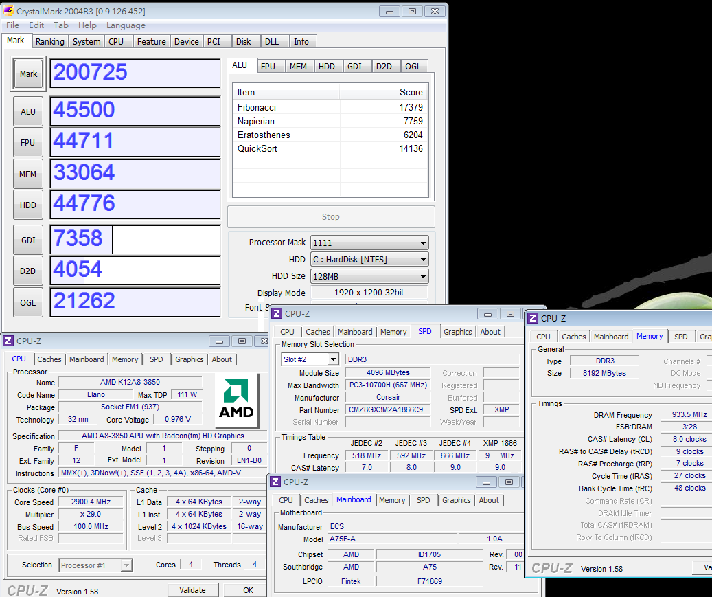
CINEBENCH R11.5
CPU => 3.46 pts
CPU(Single Core) => 0.88 pts

PCMark Vantage => 12700

Windows Experience Index - CPU 7.3

The A8-3850’s performance is little changed from the previous generation Phenom II, even when the CPU cache sizes of both L2 and L3 are slightly different.
For those who need quad-core CPU performance, AMD offers better cost to performance,
but regarding the single-thread performance of AMD CPUs, I still feel that in the future, AMD still has a lot of room to improve
DRAM Bandwidth
DDR3 1866.8 CL8 9-7-27 1T
ADIA64 Memory Read - 9360 MB/s
Sandra Memory Bandwidth - 15775 MB/s
MaXXMEM Memory-Copy - 10680 MB/s

This is where the Llano APU platform has made progress. The CPU default is adjustable up to DDR3 1866, which is a bit higher than the previous 1600 platform.
While the bandwidth and their platform have made a bit more progress, compared with rivals such as the Sandy Bridge platform, the bandwidth seems to be lagging further behind ...
DDR3 bandwidth is where AMD needs to improve in the future, and we hope that performance will improve with the launch of the Bulldozer
Temperature Performance (room temperature about 26 degrees)
Standby - 18

CPU at Full Speed - 39
LinX 0.6.4

In a test of the AMD C&Q power-saving technology, in standby the CPU clock / voltage drops significantly, and for this reason the temperature falls quite a bit
At this point, the obtained data was quite good, and even at full speed it was only 39 degrees.
However, because the chips tested for temperature on each motherboard were different, actual temperatures may have been higher for some.
But what is certain is that AMD used 32nm for the A8-3850, so there has been some progress with the temperature performance of the AMD platform
-
In early July, AMD launched the latest architecture Llano APU.
Since the launch, it has already been two and a half months. Initially, the only CPUs that can work with it were the relatively high-end A8-3850 and the A6-3650.
The market prices of course were a bit higher.
For chipsets, there are two options, the A75 and the A55, adopting the latest FM1pinout design. For now, it appears the price difference between the two is not very wide.
The main advantage of the A75 is its support for the new SATA3 and USB 3.0 specifications. If you have sufficient budget, this is the better choice.

The Llano APU was relaunched in early September together with three new CPUs, and compared with the previous two, the prices are lower
With built-in GPUs, the A4-3400/A6-3500 are quite expensive compared with the A6-631, which has no GPU
Currently, a total of five CPUs support the Llano APU architecture to offer more choices for the AMD FM1 platform
To begin, windwithme has shared tests of the previous two Llano APUs, and we know that the biggest advantage of this platform lies in its significant 3D performance.
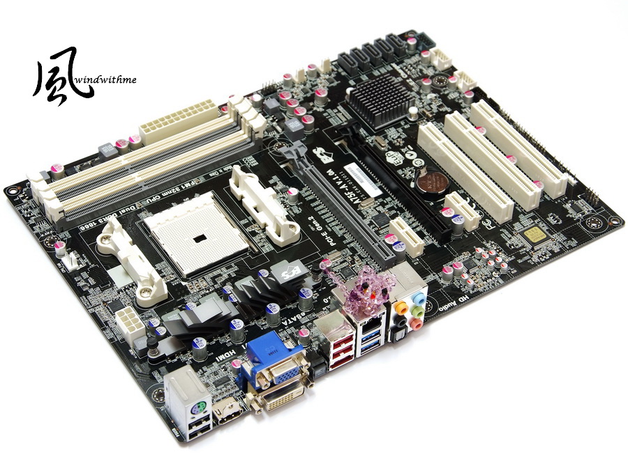
Now the star of the show is the latest product from ECS, the ECS A75 motherboard
The product is positioned as part of the Black Series, and the complete serial number is A75F-A, including the AMD A75 chipset
The PCB is black, and the extension card slots are a complimentary gray or white
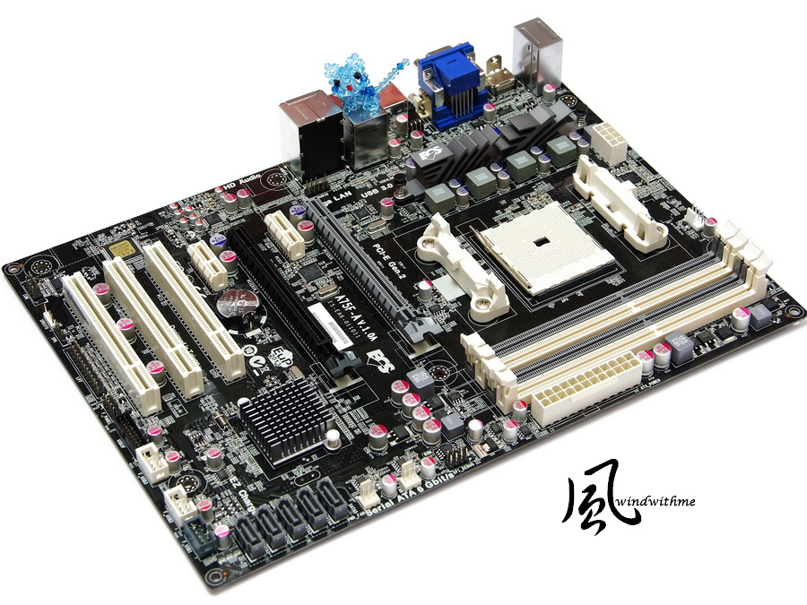
Based on the ATX form factor, the size is 305mm x 220mm, a little smaller than standard ATX measurements
The A75F-A is positioned as a high level A75 product, but the price is actually lower than many other brands
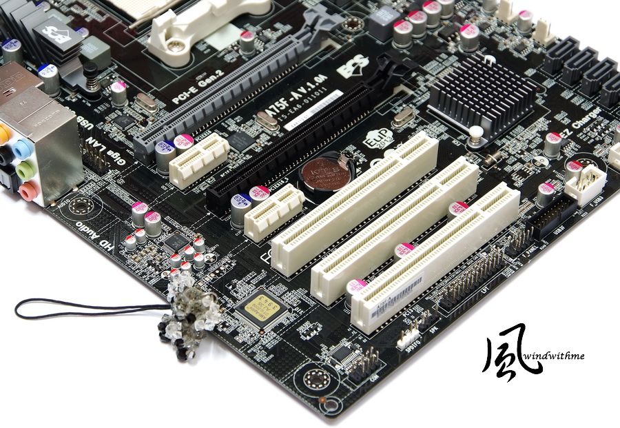
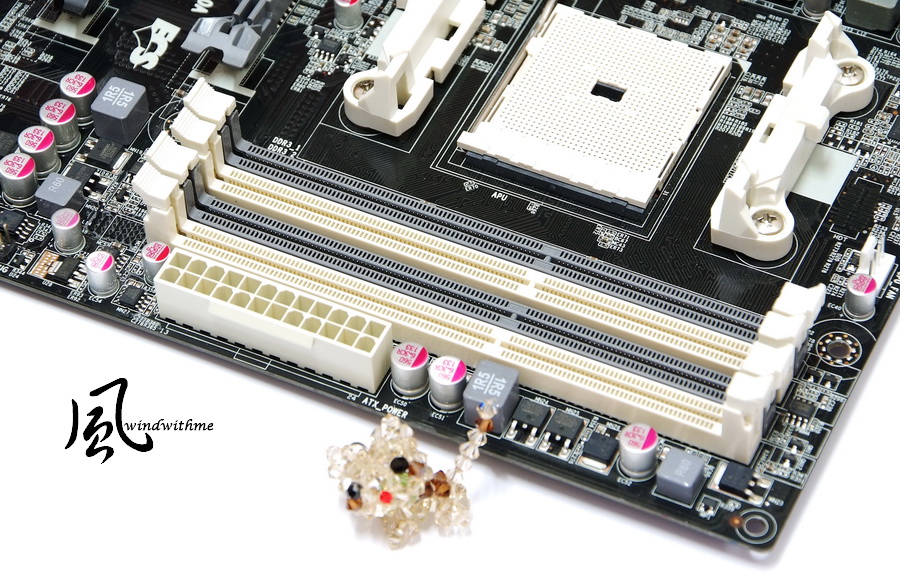
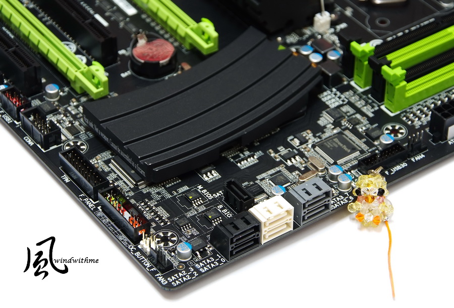
Motherboard Lower Left
2 X PCI-E X16, supporting 2Way CrossFireX technology, bandwidth of X16 + X4
2 X PCI-E X1
3 X PCI
Realtek RTL8111E LAN chip
Realtek ALC892 audio chip, with support for 8-channel High Definition Audio technology
Lower Right of Motherboard
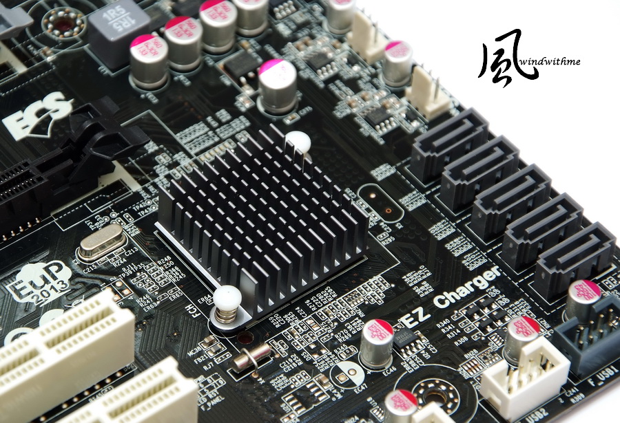
6 X gray SATA, A75 chip included, SATA3 specification, supporting RAID 0, RAID 1 and RAID 10
Lower area F_USB1 USB 3.0 expansion slots for the front

Top Right of Motherboard
4 X DIMM DDR3, supporting 1333/1600/1866/2133 (OC)
This board can be overclocked to extra performance of DDR3 2133.
Beside this is the 24-PIN power input.
Upper Left of Motherboard
The A75F-A uses a 4-phase power supply supporting AMD's latest FM1 series CPU
At the top is the 8 pin power input, and heat sinks used with the previous AM2 + / AM3 can also be installed on the pins of the FM1
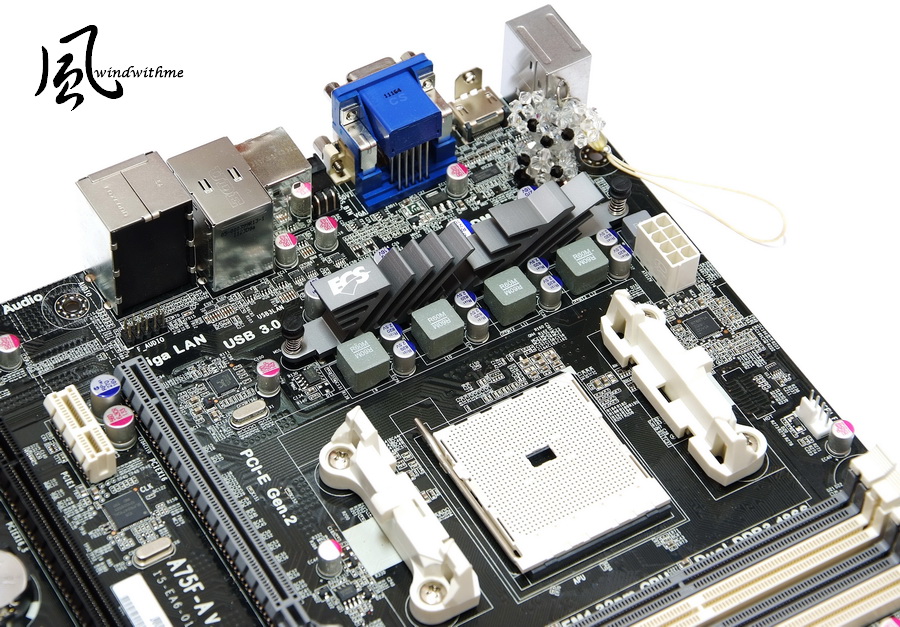
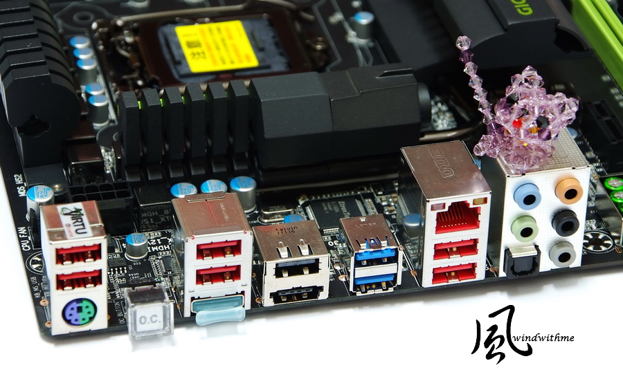
IO
1 X PS2 keyboard / mouse
VGA / DVI / HDMI
Clr CMOS button
4 X USB 2.0 (Black / Red)
1 X eSATA / USB 2.0 both supported (red)
2 X USB 3.0 (Blue)
1 X RJ-45 network connector

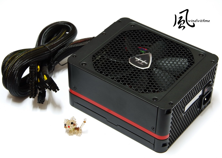
Closeup of Power Supply
While the machine is running, you can feel the temperature is not high around the heat sink.
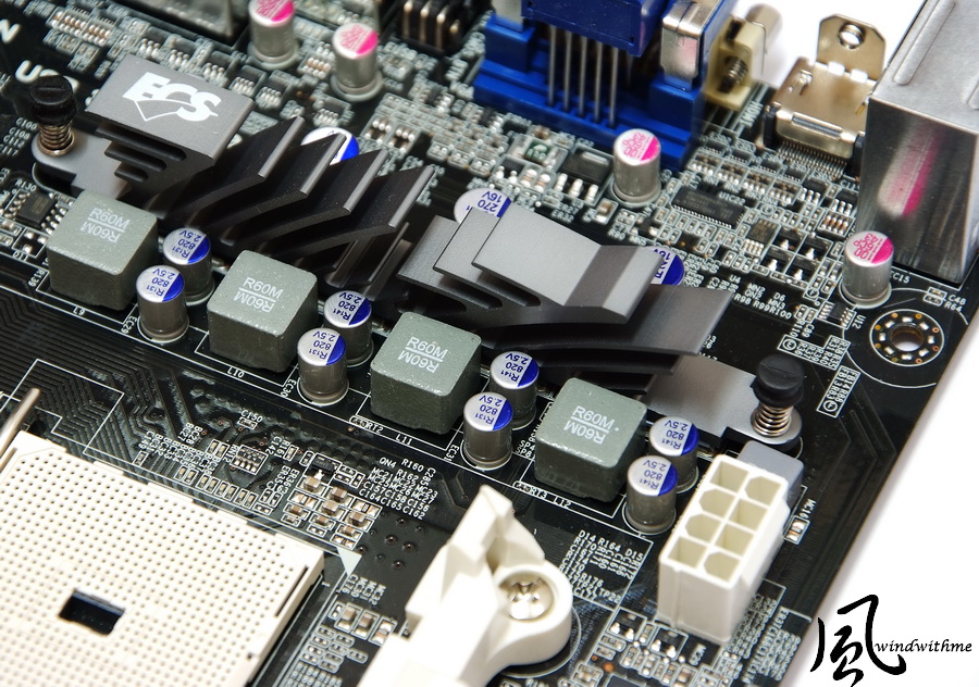
The heat sink models used with the A75F-A are of a typical style with a design that increases the cooling area
If you touch the heat sink, you’ll find the actual surface temperature is quite low, but if you use a more attractive heat sink, it’s certain to have a stronger selling point
-
CrystalMark 2004R3 => 341127

CINEBENCH R11.5
CPU => 9.74 pts
CPU(Single Core) => 2.03 pts

Windows experience index - CPU 7.8
PCMark Vantage => 24126
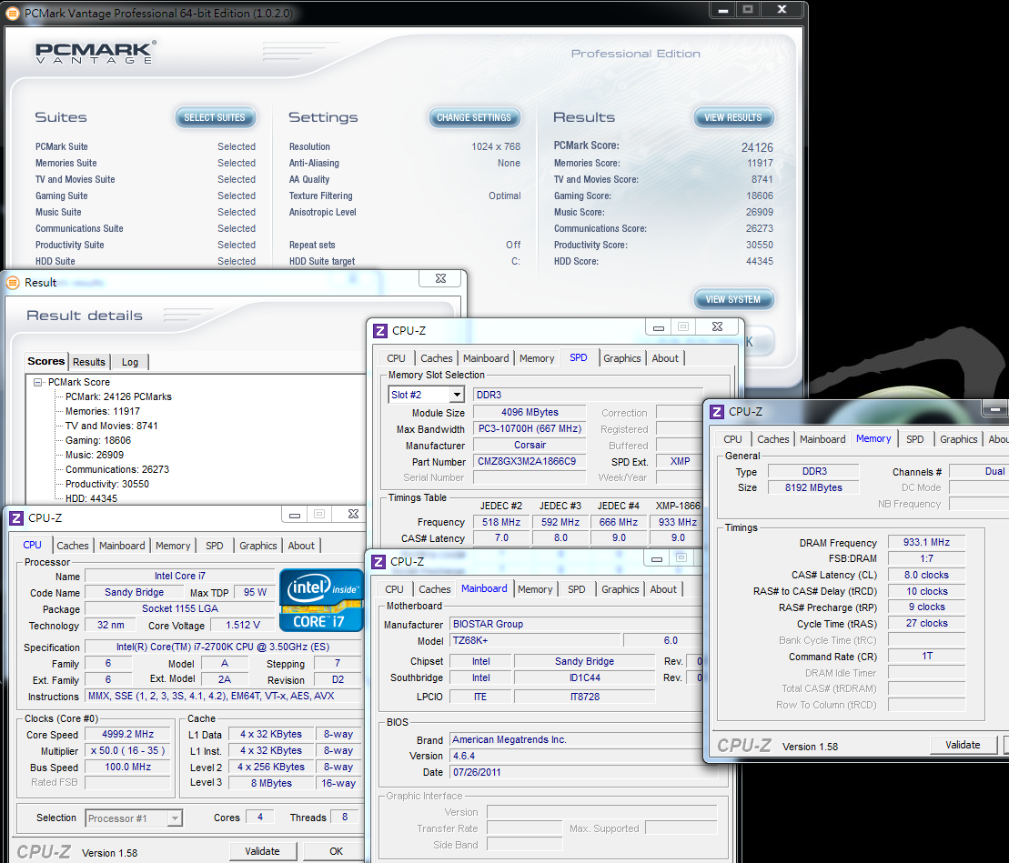
After overclocking, the performance is increased by about 30% at the single-core threading, and by over 40% at the multi-core threading, which is quite satisfactory.
The 5GHz which is the performance of 2700K should be the acme of the 4 Cores CPU on the market currently.
In the future, it may be surpassed by Sandy Bridge-E or Ivy Bridge to be released next year which uses its own LGA 2011 platform.
DRAM bandwidth test
DDR3 1866.4 CL8 10-9-27 1T
ADIA64 Memory Read - 22805 MB/s
Sandra Memory Bandwidth - 24680 MB/s
MaXXMEM Memory-Copy - 25963 MB/s
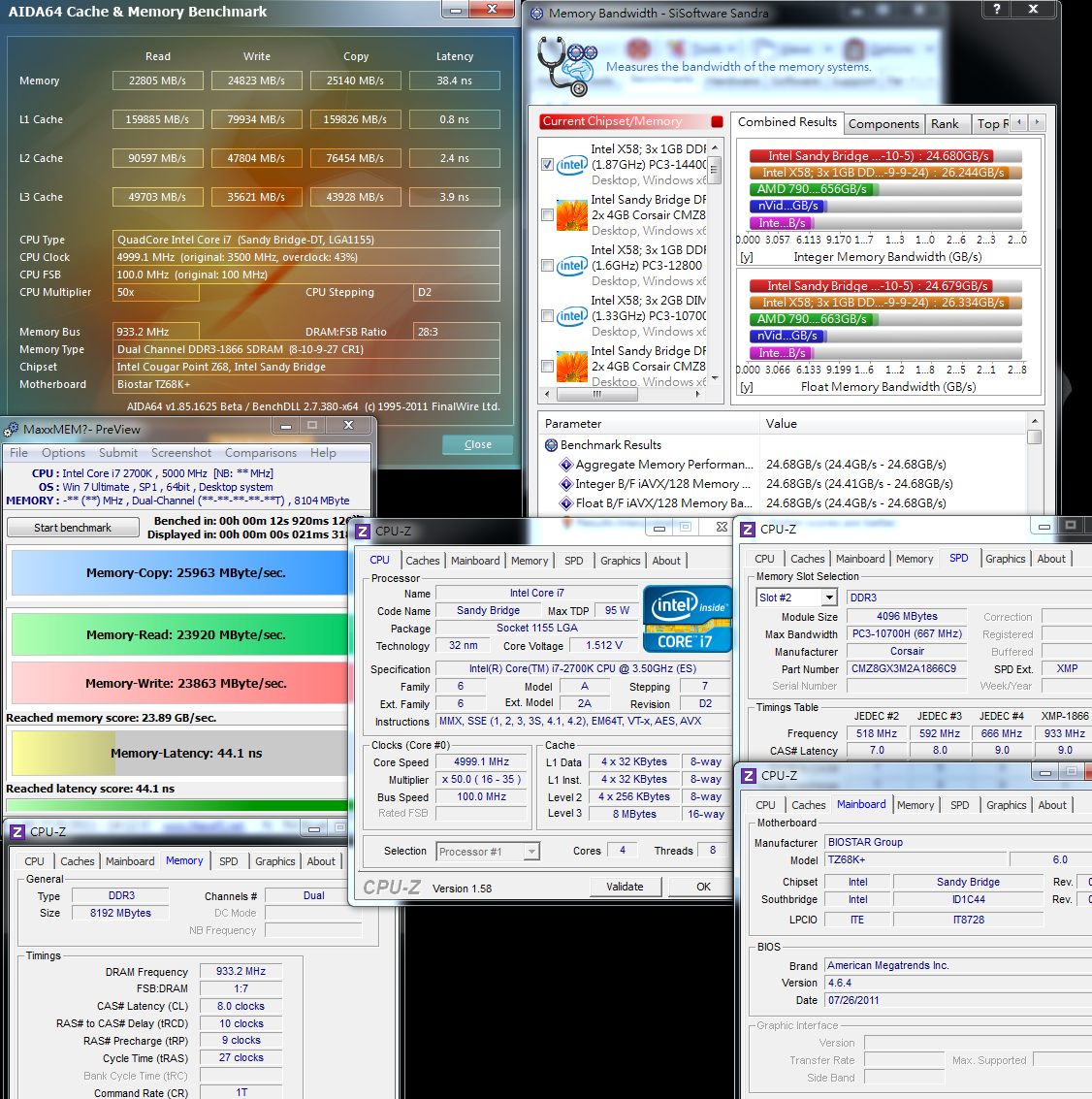
The Sandy Bridge framework improves the bandwidth of DRAM a lot, thus a dual-channel platform can already compete with the performance of a tri-channel platform of X58.
Furthermore, the bandwidth improvement for DDR3 is in clock rate, there is 10-20% bandwidth improvement after being increased from 1600 to 1866.
The high bandwidth performance for LGA 1155 is helpful to improvement for system performance to some extent.
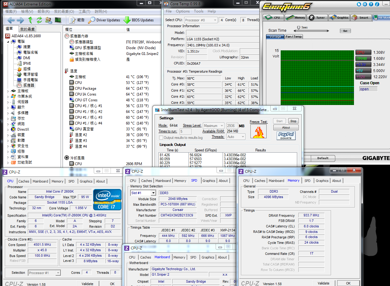
Temperature performance (about 26 DEG C at room temperature)
System standby- 36~42

CPU full speed - 76~80
Intel Burn Test v2.4,Stress Level Maximum

The temperature increases a little when system standby because of overclocking, which is substantially within an acceptable range.
The temperature increases a lot at full speed, which will also happen to the Sandy Bridge framework at the high clock rate of 5 GHz.
Therefore, it is quite important to lower the temperature which is also a challenge for the capability of the heat sinks.
The temperature is about 90 DEG C when top-level air cooling is employed previously.
The hydro-cooling performance of CORSAIR H80 is excellent, in which the temperature is below 80.
It is an acceptable overclocking temperature for most users.
For BIOSTAR, the voltage control of CPU can be strengthened, 1.512V at standby and 1.416V at full speed are helpful to stability after overclocking, but it fluctuates strongly.
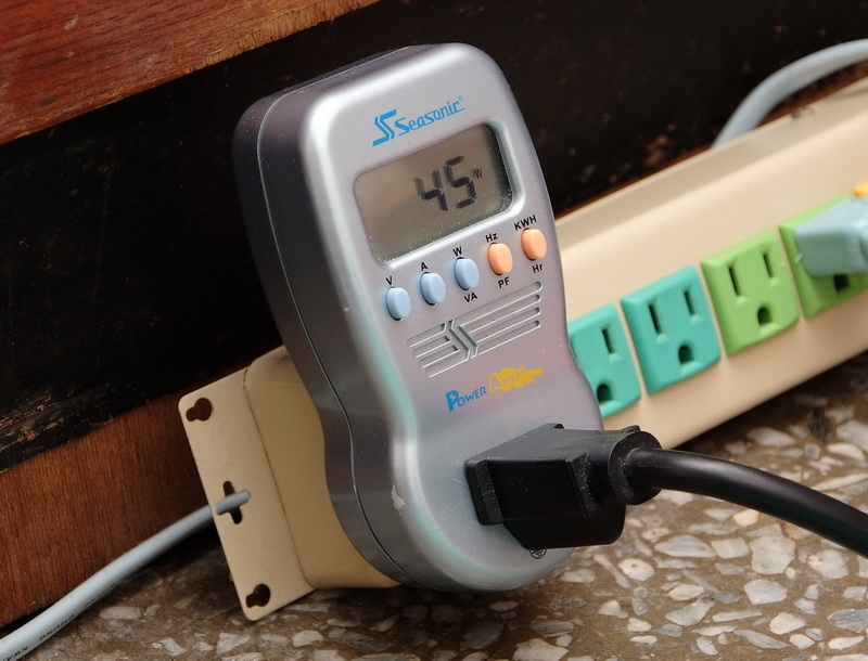
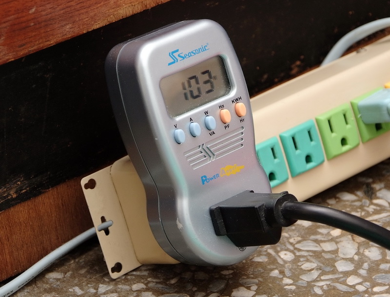
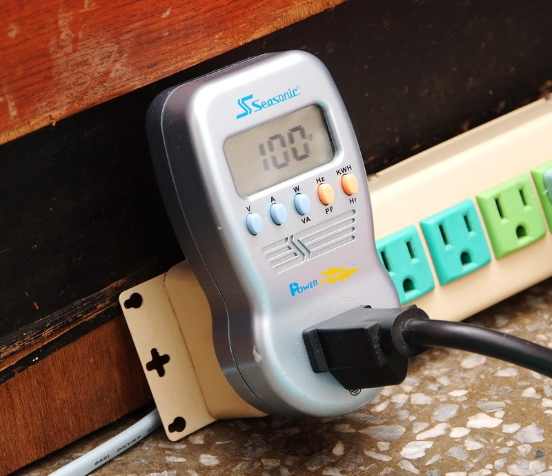
Power consumption test
No software running on OS desktop - 103W
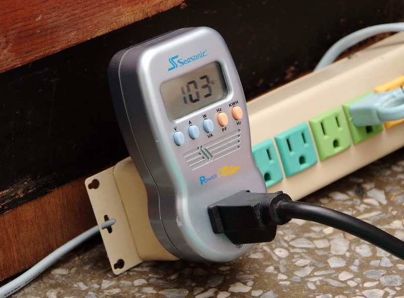
CPU full speed- 239W

After powering off the C1E, the power consumption after overclocking is increased a lot simultaneously, which it is over 100W at standby.
The power consumption will be increased by about 136 W at full speed.
From the clock rate and performance of 5 GHz, the power consumption is a little higher than 95 W which is the official preset data.
However, compared with the high power consumption of competitor’s 32 nm 4Cores/8Cores, the power consumption for 32nm process of Intel is excellent.
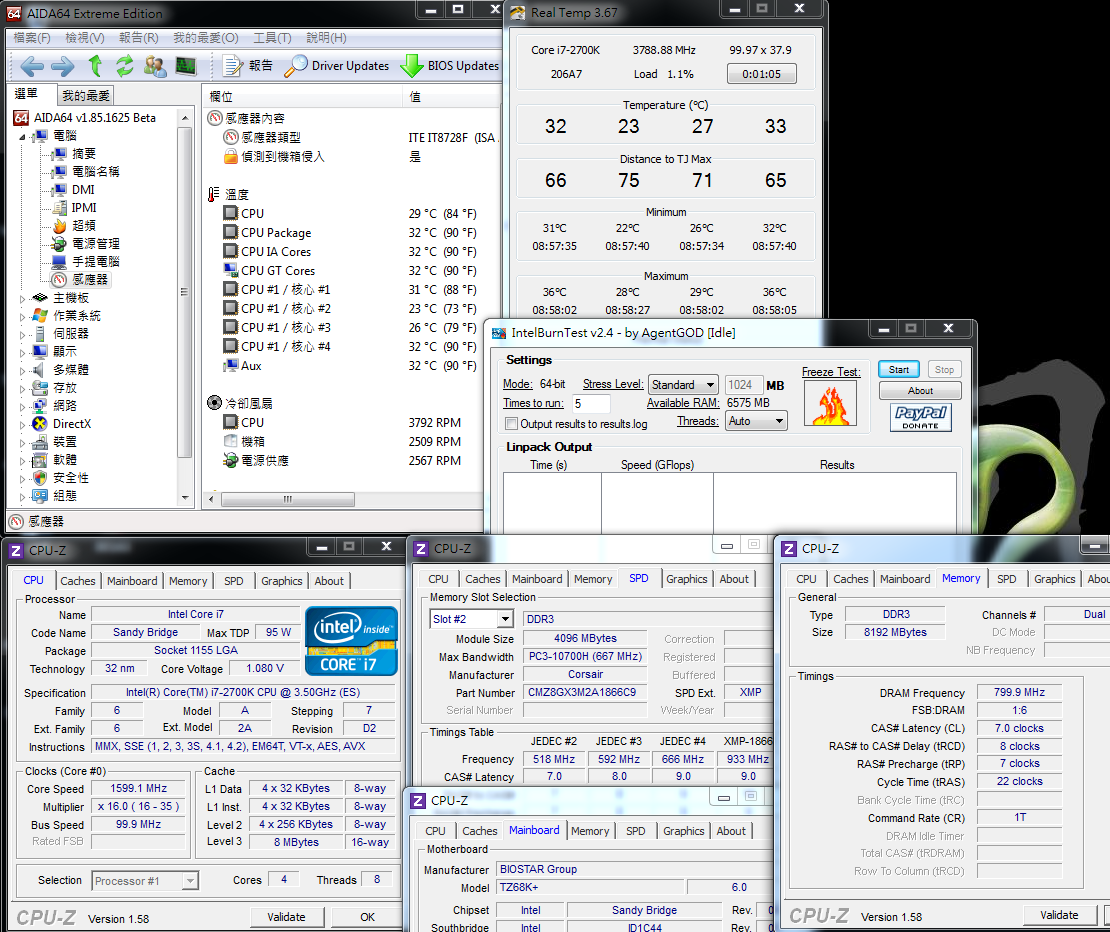
It is necessary to select two chipsets, i.e., P67/Z68 and the like to play the overclocking performance of the three frequency-unlocked CPU, i.e., 2500K、2600K and latest 2700K.
P67 has lowered to a reasonable price on the market, so that it is a MB choice with light economic burden for consumers with limited budgets.
But Z68 has the primary functions of two chipsets at the same time, i.e., overclocking frequency multiplication of CPU of P67 and display output of H67,
so that it is the chipset of LGA 1155 that has the most comprehensive functions currently.
Unlike LGA 1156 or LGA 775 at a quite high price when just released in one year, Z68 of the LGA 1155 platform soon after being put on the market has a reasonable price.
Additionally, Z68 has exclusive SSD acceleration, so that it is a good function for accelerating the performance of system for the users with small-capacity SSD on hands.
If selected by myself, I prefer to directly selecting Z68 MB optimally through adding some budgets.
The price of TZ68K+ of BIOSTAR is about the same as that of P67 of the other brands; from this part, the value of C/P is obviously enhanced.
With the overclocking capability of a rather high level and the advantages of supporting UEFI user interface and eight-phase power supply, the Z68 should be taken into account.
If the number of USB 2.0 can be increased or the voltage of CPU can be suppressed, it will be a valuable high-performance Z68 MB.
Intel will release 2700K in Q4, which should be used to replace 2600K that is the highest-level CPU of LGA 1155 currently.
Although, 2700K is only increased by 100 MHz, the price is only tens of dollars higher according to information on Internet.
The voltage for overclocking at 5GHz is about the same as that for 2600K which is shared by windwithme, and is about 1.4V.
At Nov., Intel will release a higher level LGA 2011 platform, in which the configuration of X79 and CPU will be much more expensive than that of 2700K and Z68.
On the current market, the middle-high level platform with higher value of C/P consists of several combinations, i.e., Z68+2500K or 2600K/2700K.
Personally, I think it is unnecessary for the users who already have 2600K to upgrade, and it would be better for those who want to buy 2600K recently to wait the market information of 2700K.
The above is about sharing my experience for overclocking of i7-2700K, which is provided for users in need as references.
This article is also post in my own blog WIND3C Welcome your visit.
-
Performance test for Intel HD Graphics HD3000
The preset value of GPU at BIOS is 30 which is equal to 1500 MHz after conversion.
3DMark Vantage => P2500

StreetFighter IV Benchmark
1920 X 1080 => 30.58 FPS

In the Sandy Bridge, two GPUs, i.e., HD2000/HD3000 are built in by Intel, thus the performance is much advanced than the previous edition.
The detailed test data are shared in several related articles shared by me recently (windwithme).
The HD3000 has about 6-7 times 3D performance of the previous platform built-in GPU of Intel, thus it is believed that the applicable range is wider.
The following part is about sharing of the overclocking for 2700K.
New-style UEFI graphical interfaces are introduced into the BIOS items by BIOSTAR.

O.N.E debugging page
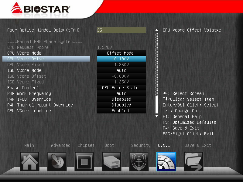
By changing 2700K at Turbo Mode to 50, the clock rate, i.e., 100 X 50 => 5GHz, will be executed.
The Internal PLL Voltage Override is a special Intel overclock option, which effectively strengthens the stability of the CPU after substantially overclocking.
It is suggested that the C1E should be powered off when overclocking, thereby facilitating control of clock rate and voltage of the CPU.

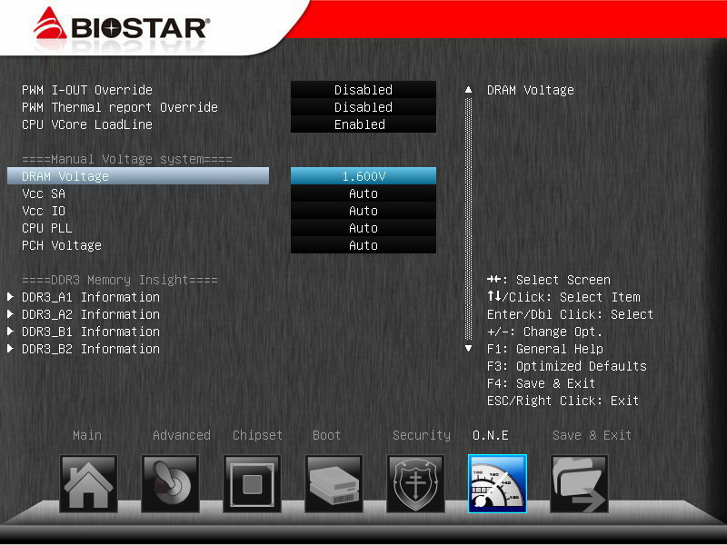
When setting clock rate and parameters for DRAM, the smaller the numerical values are, the higher the performance is.
The following example is DDR3 1866 CL8 10-9-27 1T, and the set values for the other detailed options are adjusted for optimization.
User can perform miniature adjustment on the clock rate or the parameters according to the condition of the DDR3 on hand, so as to increase the performance of the DRAM.

The CPU voltage adjustment is one of the key points for overclocking.
It can be adjusted according to the condition of CPU and the heat-dissipation system of the platform; and the CPU VCoce LoadLine is Enabled.
The DRAM voltage is another option to be adjusted for overclocking.
Substantially, the overclocking at the Sandy Bridge platform is much simpler than that of the previous platforms,
so the overclocking can be realized by grasping CPU frequency multiplication, DDR3 parameters, and voltage adjustment for both.
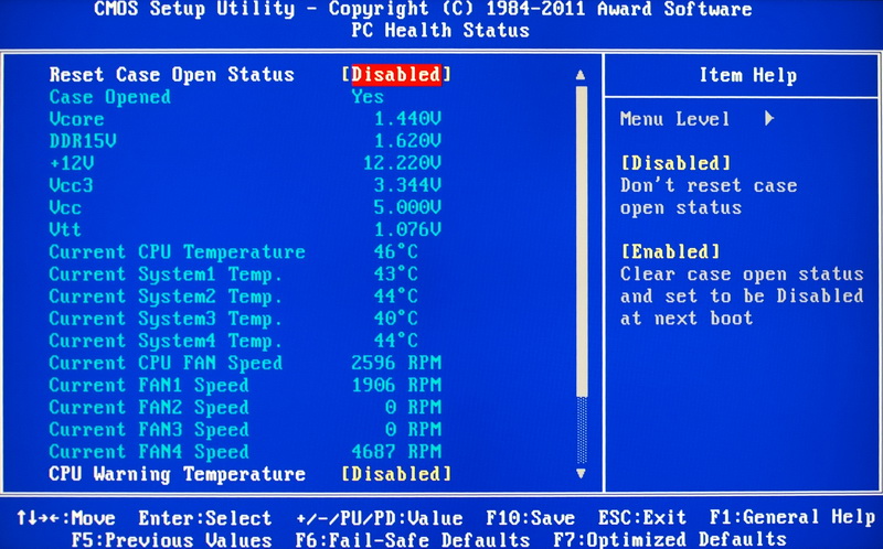
PC Health Status
It’s still felt that the temperature test result for CPU is on the much higher side;
actually, the wind temperature of the heat sinks or the temperature of the software for measuring temperature are much lower.

The above are personally stable set values for 2700K OC 5GHz, which may be readjusted for overclocking according to different hardware or difference between conditions individually.
However, the general direction is at least right, which can be considered as reference for setting BIOS for the overclocking users.
Overclocking performance
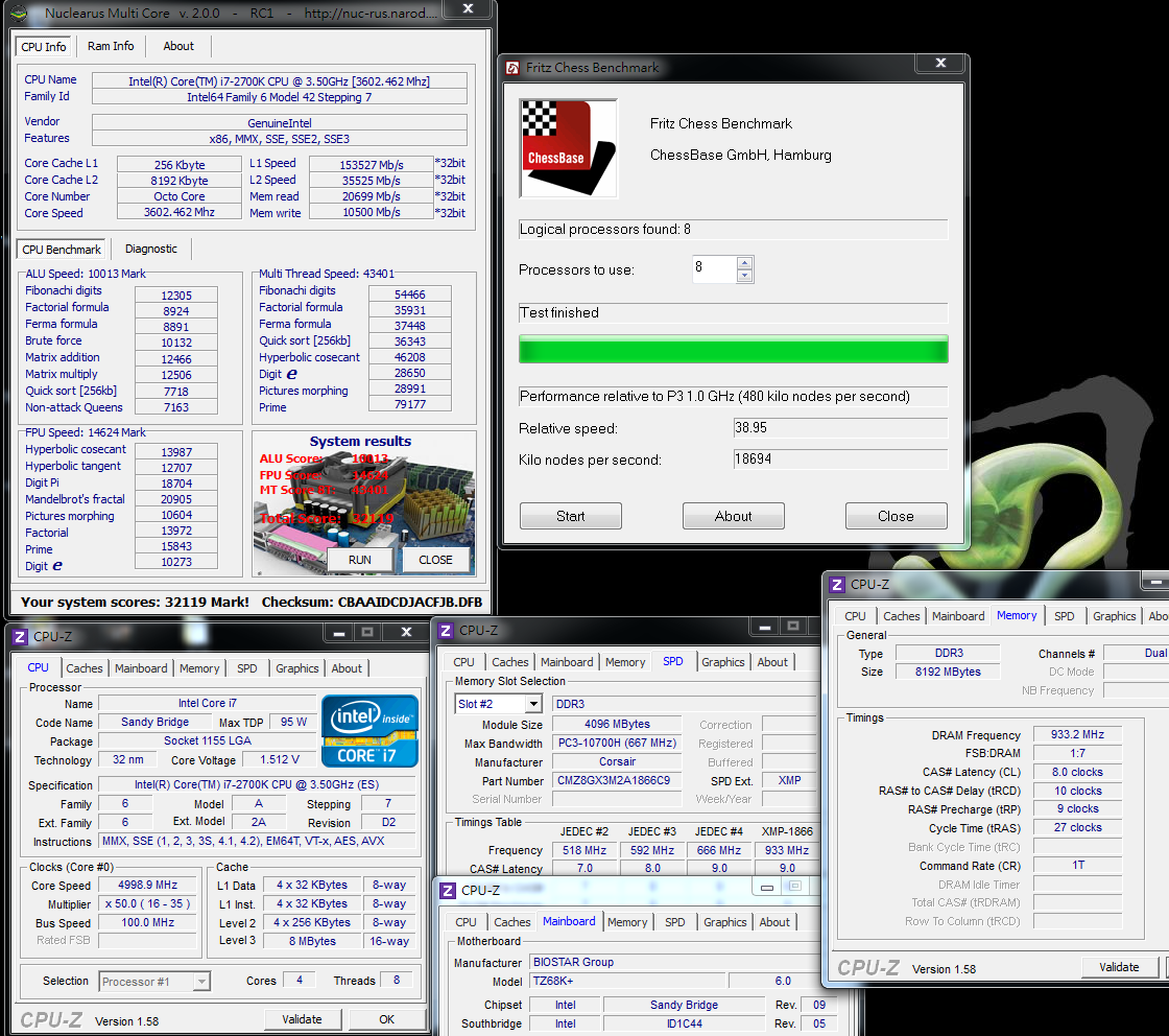
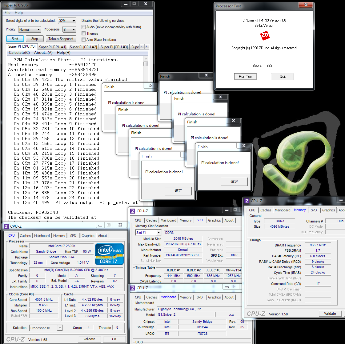
CPU 100 X 50 => 4998.9MHz, at full speed is 1.416V.
DDR3 1866.4 CL8 10-9-27 1T 1.600V
Hyper PI 32M X 4 => 11m 52.875s
CPUMARK 99 => 771
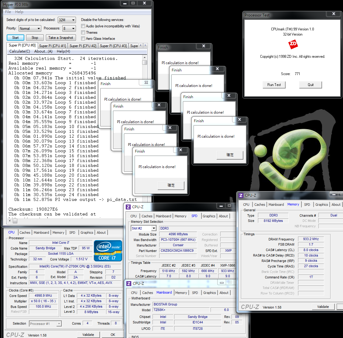
Nuclearus Multi Core => 32119
Fritz Chess Benchmark => 38.95/18694
-
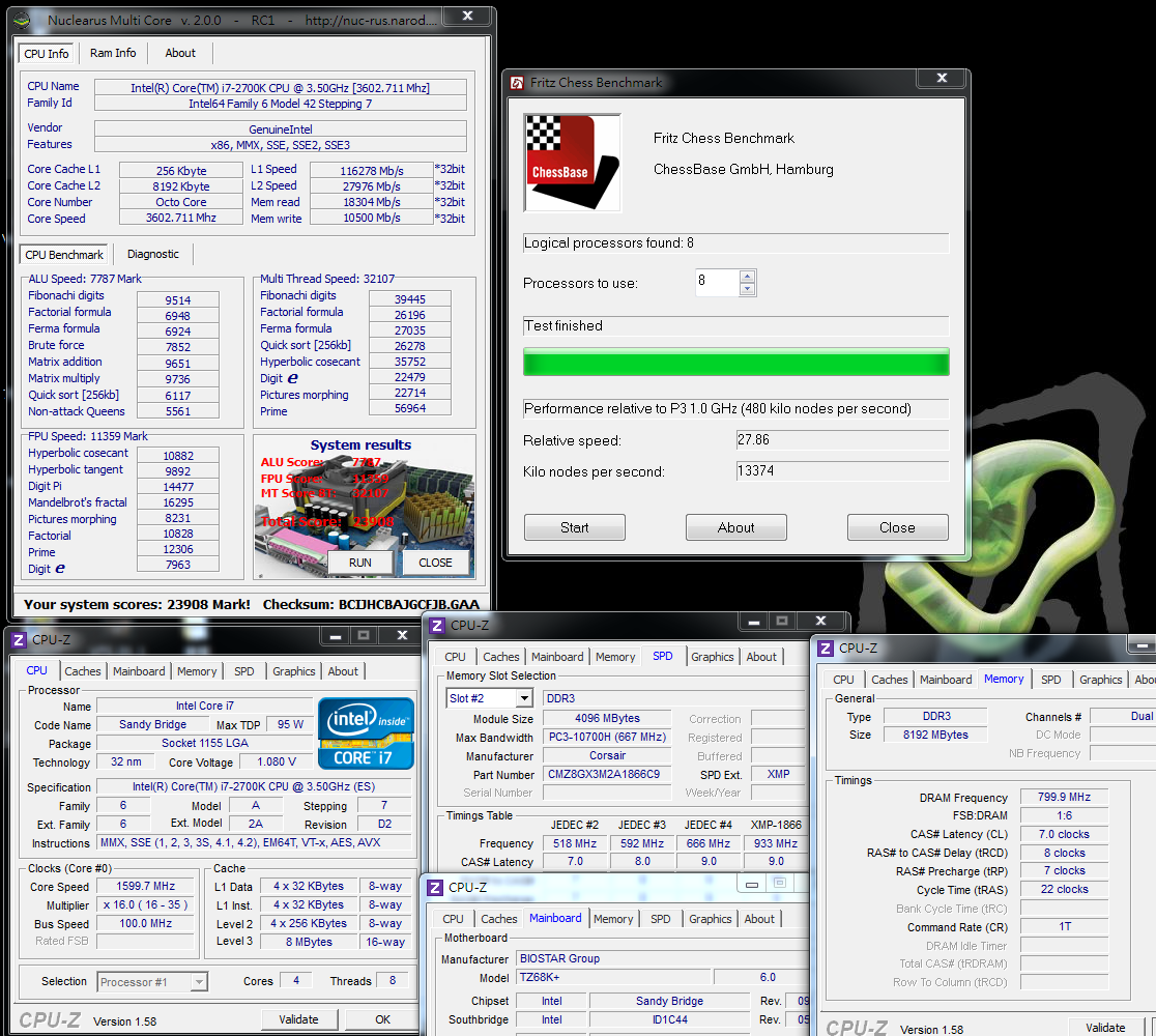
Nuclearus Multi Core => 23908
Fritz Chess Benchmark => 27.86/13374
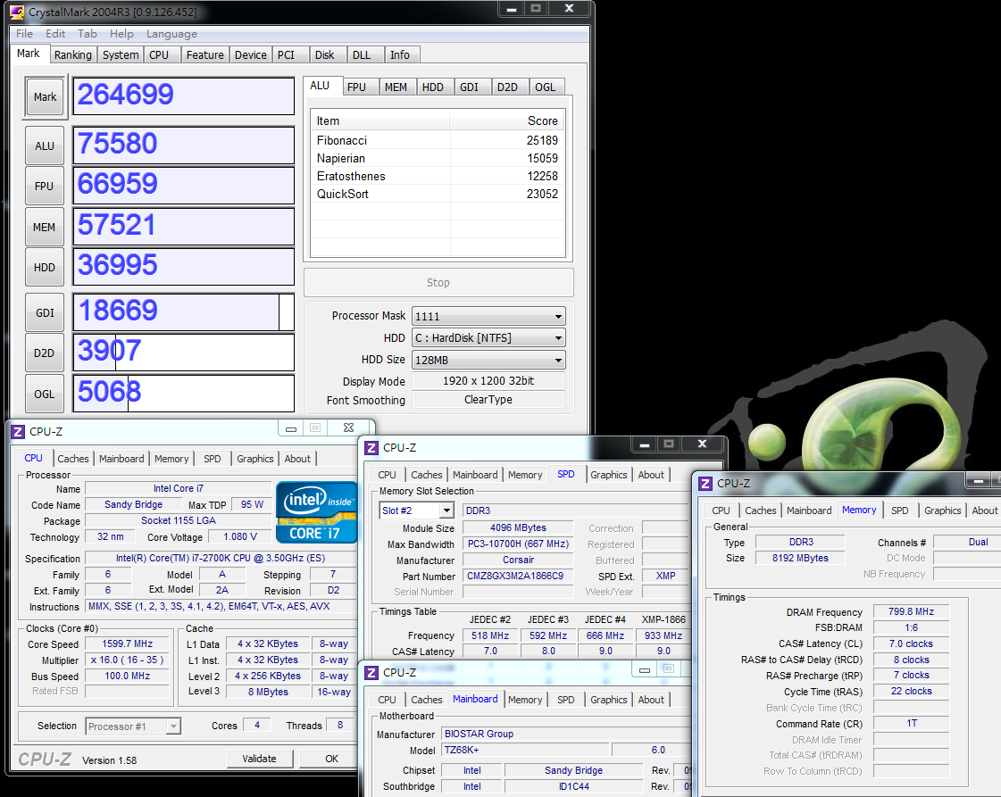
CrystalMark 2004R3 => 264699
CINEBENCH R11.5
CPU => 6.93 pts
CPU(Single Core) => 1.57 pts
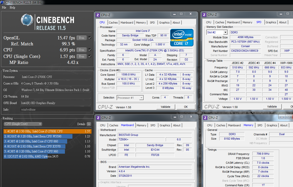
Experience index of Windows- CPU 7.6

PCMark Vantage => 19386

The frequency multiplication of the 2700K in the mode of Turbo Boost 2.0 is 39, 38, 37 and 36 respectively; and the basic clock rate is 3.5 GHz.
The above specification is 100 MHz higher than that of the 2600 K, the performance of this part is presented in the test, but the improvement is not much.
Practically, both the 2600K and the 2700K are the highest-level CPUs in the framework of the Sandy Bridge, and the data obtained without overclocking is fairly high already.
For a general use environment, most of the software requirements can be met by using the high performance preset in 2700K.
DRAM bandwidth test
DDR3 1599.8 CL7 8-7-22 1T
ADIA64 Memory Read - 19618 MB/s
Sandra Memory Bandwidth - 21335 MB/s
MaXXMEM Memory-Copy - 21168 MB/s

The DDR3bandwidth is much higher than that of our own platform or a competitor’s platform, which is the advantage of the improved LGA 1155.
The high transmission performance of nearly 20000 MB/s can be achieved only by using DDR3 1600, and the voltage is lower than that for the previous platforms.
Temperature performance (about 26 DEG C at room temperature)
System standby - 23~33
CPU full speed - 40~46
Intel Burn Test v2.4,Stress Level Maximum

The temperature performance when system standby is good by enabling the energy-saving function of C1E.
With the latest Hydro Series H80 of CORSAIR and the high thermal diffusivity of the hydro-cooling framework, the temperature is only 46 DEG C at full speed.
Only by working with excellent air-cooling or hydro-cooling equipment, the state of the preset value on 2700K can still be lowered to a low temperature.
Power consumption test
No software running on the OS desktop - 45W
CPU full speed- 103W
Due to introduction of 32nm, the power consumption is much lower than that of the previous generation Core i7-870 with the process of 45nm.
The power consumption of the clock rate at the environment of C1E is only 58W higher than that of the preset maximum clock rate.
Based on several articles about AMD APU shared by me recently, in a test with the same 32 nm and 4Cores, the power consumption of the APU platform is nearly twice that of AMD.
It is thus clear that the performance and the power consumption under the Intel’s framework have good advantages under the same process.
-
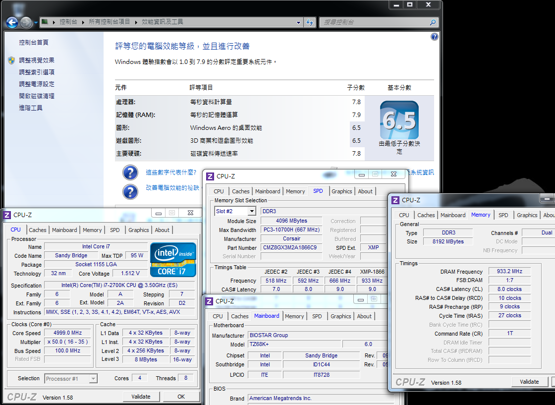
Intel released the new generation framework of Sandy Bridge at early January, 2011; meanwhile, LGA 1155 is provided for support.
Compared with the specifications of several platforms in the past, the LGA 1155 is provided with a lot of modifications in CPU overclocking (OC) at this time.
Firstly, when a CPU with the external frequency of 100 MHz is overclocking, the other surrounding clock rates will be increased accordingly, thus the upper limit will fall around 110 MHz.
Although the new 32nm process is introduced into the new generation 4 cores CPUs, overclocking can be only achieved by using frequency multiplication.
The model names of i5-2500K and i7-2600K that are two kinds of CPUs without lock frequency multiplication have been released for a long time, which are considered as the representatives of the overclocking line.
However, the overclocking can be only done by working with the chipset of overclocking frequency multiplication, i.e., P67 or Z68.

The overclocking environment for LGA 1155 is simply declared above, hoping the users can aware of the hardware for the equipment clearly.
The middle-level CPU featured by overclocking is Core i5-2500K, while the advanced-level is Core i7-2600K.
The main difference between them is that the 2600K is provided with Hyper-Threading (HT) technology and an 8MB L3 cache, while the 2500K is only provided 6 MB L3 cache without HT.
This time I pursue Core i7-2700K which will appear on the market very soon and replace the advanced 2600 K.
The total clock rate of 2700K is 3.5 GHz, which supports the new generation Turbo Boost 2.0 and can reach the maximum performance of 3.9 GHz.
The real 4 Cores are incorporated into the Hyper-Threading technology, so that eight threading can be executed, 4C/8T for short.
With the 32 nm process, the power consumption of 95W and the 8-MB L3 Cache, the 2700K, surpassing the 2600K 100MHz, becomes the most advanced CPU of LGA 1155.
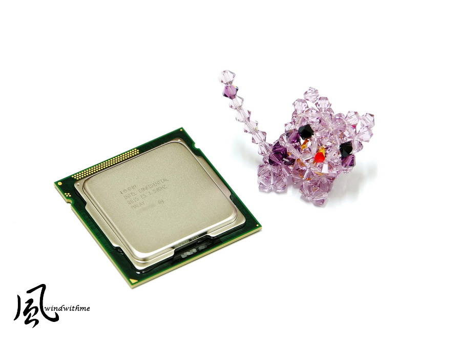
The rear side of the 2700K is still D2 Revision, so that there is little difference in appearance between the 2700K and the 2600K at this part.

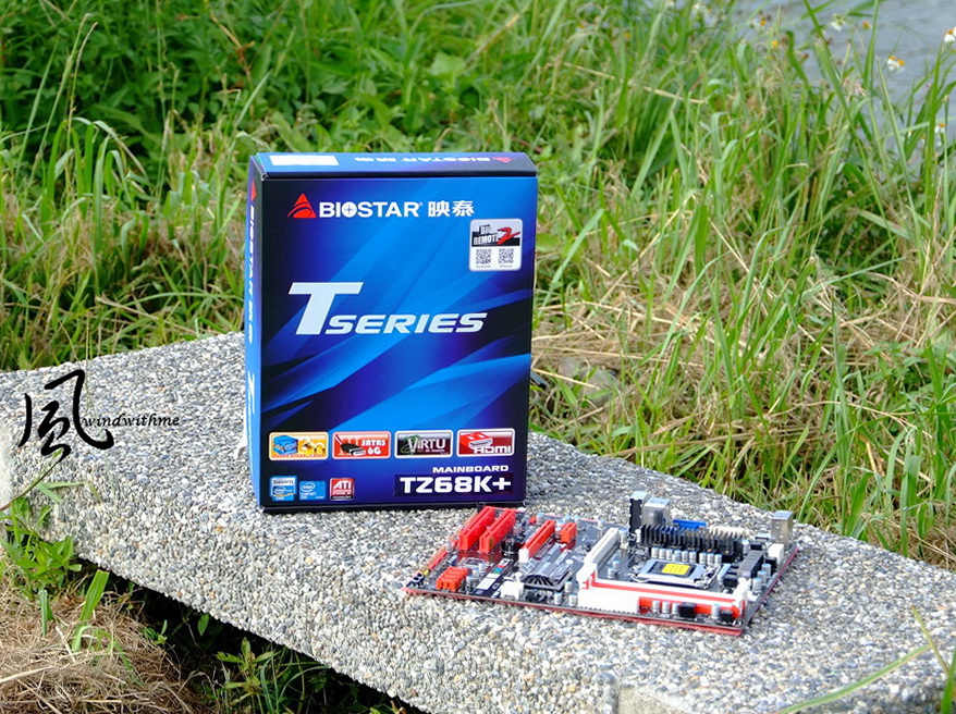
The MB is the latest Z68 high-level chipset of LGA 1155, i.e., the latest version TZ68K+ released by BIOSTAR.
The appearance and the specification are the same as that of the TZ68A+ shared before and the primary difference is supply voltage of CPU.
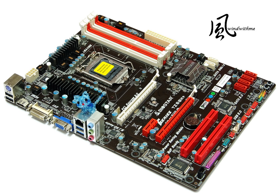
Although the TZ68K+ is the new edition of BIOSTAR Z68, the price is still about US$99, thus it can challenge the low-price market of ATX Z68.
By using the well-marked red-black matching, it has the most specifications as that of the Z68 series with the built-in Power/Reset button and a simple debugging LED.

With respect to IO, there are three types among which the two blue USBs 3.0 can provide high-speed transmission.
If provided two more USBs 2.0, it would be more perfect with respect to the scalability.

The previous TZ68A+ is designed with four-phase power supply only, while the new edition TZ68K+ is provided with eight-phase power supply, which is the primary difference.
However, as mentioned before, one-phase power supply can provide about 30-40 W, so , the four-phase power supply is already quite enough for overclocking of power consumption of Intel CPU.

The heat sinks above the Z68 chipset look good because of being cut by a special manner.
Two native SATA3 units of Z68 are positioned at the right side, which are used at a general environment or in a Raid0 state.

Test platform
CPU: Intel Core i7-2700K
MB: BIOSTAR TSERIES TZ68K+
DRAM: CORSAIR CMZ8GX3M2A1866C9R
VGA: Intel HD Graphics 3000
HD: Intel 510 Series 120GB
POWER: Thermaltake TR2 450W
Cooler: CORSAIR Hydro Series H80
OS: Windows7 Ultimate 64bit

Firstly, a performance test is performed by using the preset value of CPU.
Preset the performance
CPU 100 X 35 => 3500 MHz (booting Turbo Boost, and then C1E)
DDR3 1599.8 CL7 8-7-22 1T
Hyper PI 32M X8 => 15m 21.977s
CPUMARK 99 => 597

-
FINAL FANTASY XIV
1920 X 1080 => 4743

Due to Z68 PCI-E limited bandwidth, official spec cannot support 3Way graphics.
GTX560 Ti performance should be satisfied by most gamers.
If you need high resolution and effects, you can use 2-way SLi or higher grade VGA.
GIGABYTE G1.Sniper2
Good
1.G1.Sniper2 is G1-Killer series which has top quality packing and components.
2.Built-in Creative CA20K2 audio chip with rare Japanese made high end caps and 128MB Memory cache.
3.Killer E2100 NPU chip with 1GB DDR2 cache provides better network traffic control.
4.High end Z68 with HDMI output supports Intel IGP exclusive Lucid Virtu technology.
5.Provides exclusive Front Access Control Panel to support USB 3.0 and quick OC. It also supports audio amplifier chip.
6.Special design military style heat sink has good quality and lookgin.
Weak
1.CPU PWM should provide at least 12-phase to fit the product price.
2.No external chip to support 3Way VGA.
3.Can consider to make audio or LAN sub-card for more options. But it may cause users to have less PCI-E slots.
4.No GUI BIOS interface.
Performance ★★★★★★★★★★
Components ★★★★★★★★★☆
Specification ★★★★★★★★★☆
Appearance ★★★★★★★★☆☆
C/P Value ★★★★★★★☆☆☆
For Intel Z68 exclusive Lucid Virtu Virtualization technology and SSD speed up Smart Response technology.
I have shared in former several Z68 articles for detail introduction, using guide and performance.
Currently, entry Z68 and high end one price difference is around 1.5~2c times. The main reason is components and spec.
G1.Sniper2 positions at Gaming market. The audio and LAN chips are the top level in MB.
Now the high end MB is for OC or Gaming. G1.Sniper2 integrates both advantages.
If you buy same level audio and LAN cards, it will cost you much.
G1.Sniper2 price is top. These two hardware components can enhance the product value.
For looking for high end and OC Z68 gaming lovers, G1.Sniper2 can put into your wish list.
Former, some readers suggest me to test more mid-end product, so this year I am trying to review more mid end or entry products.
Like H61/H67, Pentium G620 and Core i5-2500K, if you are interested, you can search for that.
This review takes me over 3 days, due to take pics, BIOS set and OC fine tune.
Some readers may think it’s too long to read.
If it’s possible, I am considering to separate into 2 parts like very popular Taiwanese movie, Seedig Bale.
But after considering, I still decide to make in one article. If you are not familiar with OC or interested in buying in Z68, you can use it as your reference guide.
This article is also post in my own blog WIND3C Welcome your visit.
-
DDR3 Test
ADIA64 Memory Read - 24923 MB/s
Sandra Memory Bandwidth - 27863 MB/s
MaXXMEM Memory-Copy - 27807 MB/s
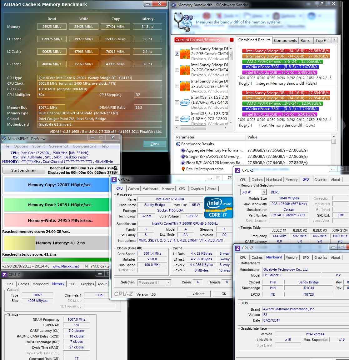
Z68 set DDR3 clock at 2133, the ADIA64 and MaXXMEM performance is over X58 DDR3 2000.
But, Z68 Sandra benchmark is lower than X58. After Sandy Bridge enhance the memory controller, the performance can compete with 3-channel.
If you want to OC LGA 1155 DDR3 to 2200~2300, you have to pull CPU clock to over 100MHz first.
Temperature Test (Room Temperature 28℃)
Enter to OS Desktop - 36~42

CPU Full Speed - 70~80
Intel Burn Test v2.4,Stress Level Maximum
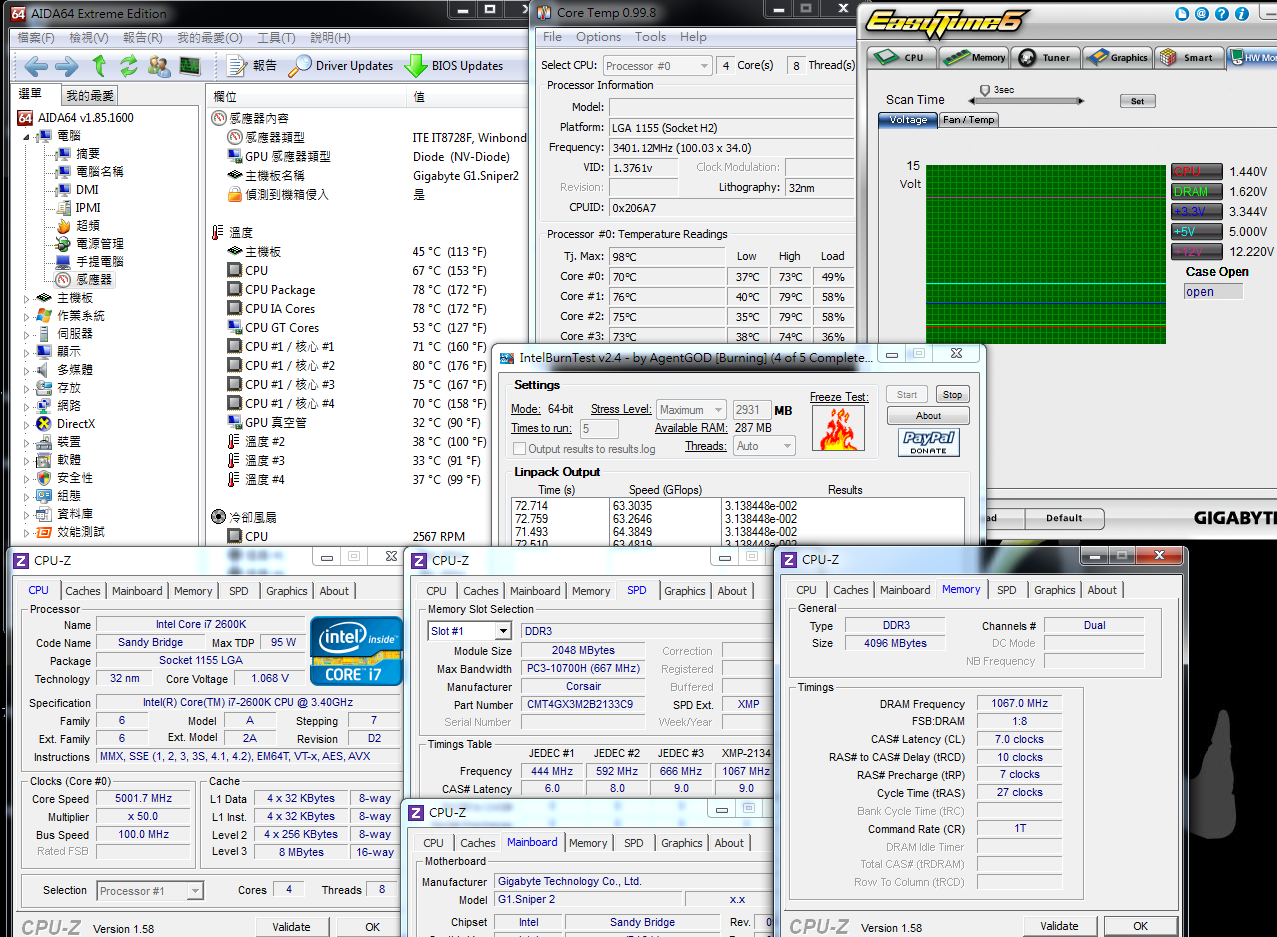
Enter to OS desktop, the temperature is not big difference. 5GHz full speed max temperature is 80 which is also acceptable.
There are 2 issues in OC, one is CPU voltage too low and the other is temperature rise due to CPU voltage too high.
It takes your time to fine tune the best CPU voltage during OC.
Using CORSAIR H80 water cooling system, the temperature is good. If it’s winter, the CPU temperature will be even lower.
Power Supply is Thermaltake high end product, Toughpower Grand Series.
Toughpower Grand Series is 80Plus Golf Certificate which is excellent performance for power saving.
TPG-1200M is highest watt version in Toughpower Grand Series. Of course, all spec is the highest.

My first impression is the shell design which is curve design.
It’s dual 12V to support 40A and 85A. The max power output is 1200W.
14” dual ball baring flower shape fan is also special. The acoustic is very quiet.
Modulized design is the must for high end Power Supply.
It’s all Japanese made electrolytic and solid caps. The official warranty is 7 years.
You can be more confident with Thermaltake.

Power Consumption Test
Enter to OS Desktop - 116W

OCCT POWER SUPPLY Mode - 468W
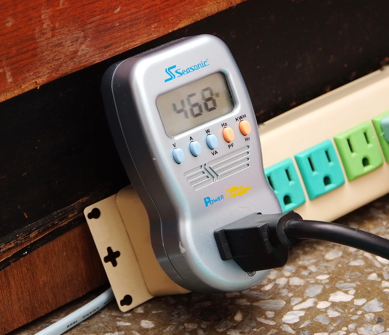
CPU voltage pull to 1.4V when OC to 5GHz, the power consumption only increase 16W when enter to OS desktop.
Full speed is only 58W higher which is acceptable range.
2600K OC 5GHz can be run stable in safe temperature range.
Some users think bigger watt Power Supply will consume more power. It’s not a right idea.
Like the same test configuration, if I use 450W PSU, the power consumption will be 14W higher.
1200W means max output watt. The power consumption level is decided by 80Plus grades.
It’s like a big pipe. The water flow amount is decided by tap. 1200W doesn’t mean it always work under max power output condition.
Higher watt Power Supply is mainly for upgradability.
My friend used 550W in the beginning and he upgraded to 750W when he started to use SLi.
Recently, he upgraded to 850W due to buy more high-end VGA.
So if you would like to reserve some upgradability for game or VGA card, I suggest you better to get higher watt PSU.
VGA is nVIDIA GTX560 Ti
3DMark Vantage => P23771
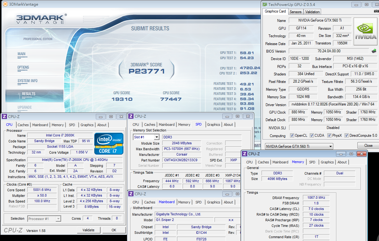
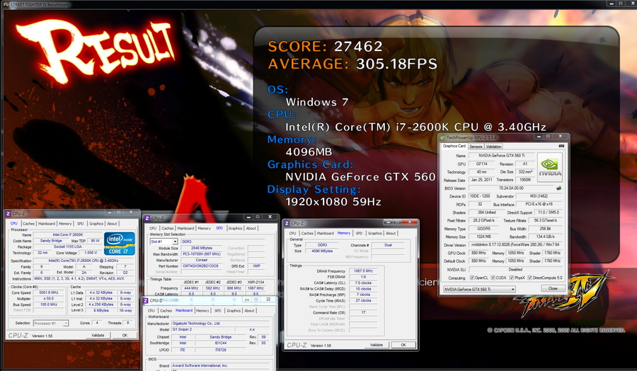
StreetFighter IV Benchmark
1920 X 1080 => 305.18 FPS
-
Clicking "Quick Boost" will enable "Smart Quick Boost" and “@BIOS" will enable "@BIOS".
These two are GIGABYTE exclusive applications. Touch BIOS integrates both for users easy to install.

Killer E2100 LAN Chipset SOftware - Bigfoot Networks Killer Network Manager
This network manager features are very rich. Users can know the network status through this software.
Upper left, EZ Smart Response, enable system HDD can switch to RAID model and enable ISRT under AHCI/IDE mode automatically.

Creative provides Entertainment, Game, Audio Creation modes.
The Game mode panel and items as right hand side. It includes rich fine tune items.
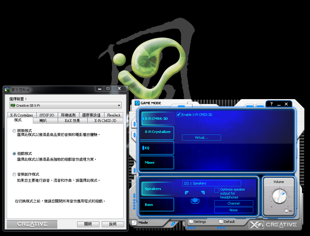
Entertainment mode panel interface is familiar to me as my X-FI audio card.
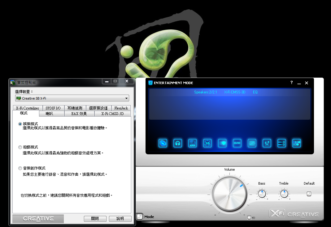
Audio Creation mode provides different panel and items.
It looks like Creative own EMU audio panel, but actually the items and features are different.

Previously, I tested the audio effect in G1 X58.
I would like to repeat some key points. X-FI audio is well benefit the video or gaming multimedia.
You can feel very good sound filed. No matter bass, fighting or demolish, it’s really shocked.
G1 builds in such high end audio chip and caps, it’s good C/P for gamers. You don’t need to buy an external sound card.
For who owns 2500K or 2600K, many people want to use at 5GHz.
However, for this high range OC, you need good quality CPU and high end cooler.
If you don’t set well, the system will be unstable and CPU will be in high temperature. 5GHz is love and hate setting.
Below is stable 5GHz OC Test
CPU 100 X 50 => 5001.4MHz 1.400V
DDR3 2134.2 CL7 10-7-27 1T 1.620V
Hyper PI 32M X8 => 12m 09.442s
CPUMARK 99 => 771

Nuclearus Multi Core => 31325
Fritz Chess Benchmark => 39.12/18776

CrystalMark 2004R3 => 400655

CINEBENCH R11.5
CPU => 9.84 pts
CPU(Single Core) => 2.03 pts

PCMark Vantage => 26169
From 4.5GHz to 5GHz, the CPU performance increase around 10~12%.
CPU performance enhance range is not much. However, 5GHz is an excellent feeling for most users.
2600K single core performance and OC range is the best in the market. The multi-tasking performance is only behind 6C12T 980X and 990X.
AMD will launch 8-core CPU in the future, called Bulldozer. Its multi-tasking performance may be higher than 2600K.
-
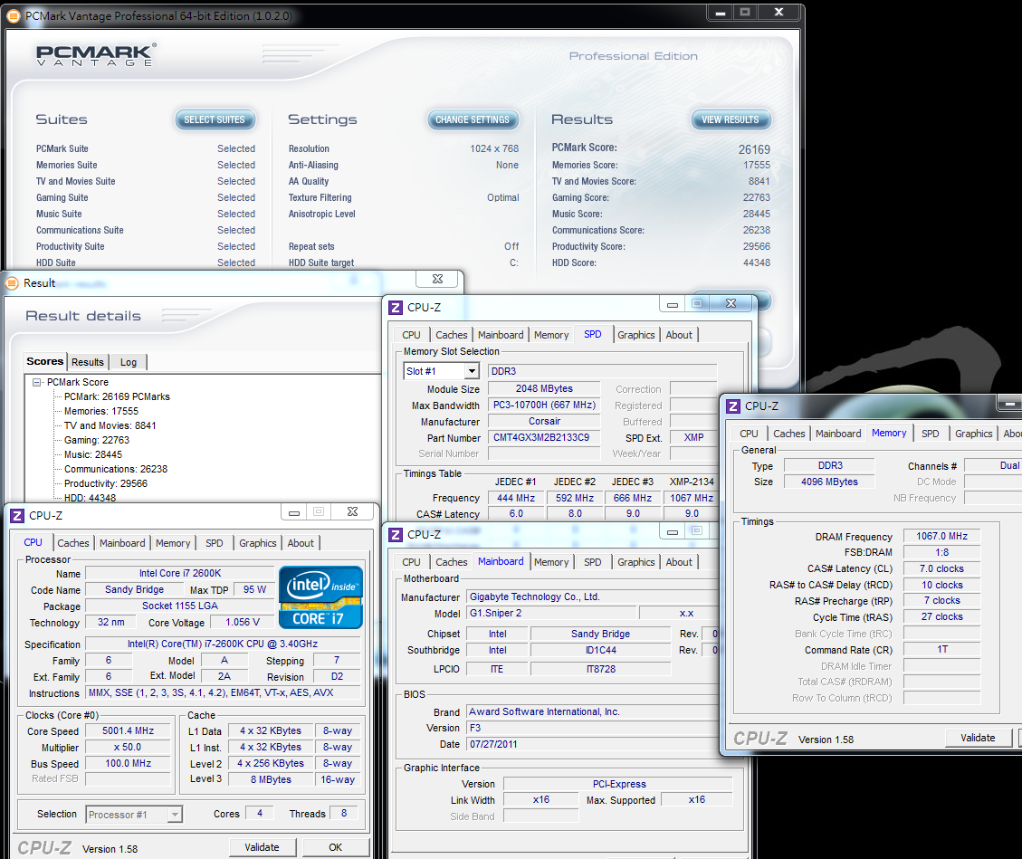
CrystalMark 2004R3 => 381995
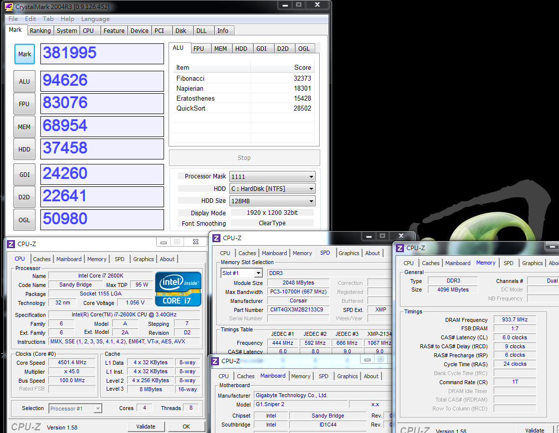
CINEBENCH R11.5
CPU => 8.80 pts
CPU(Single Core) => 1.83 pts
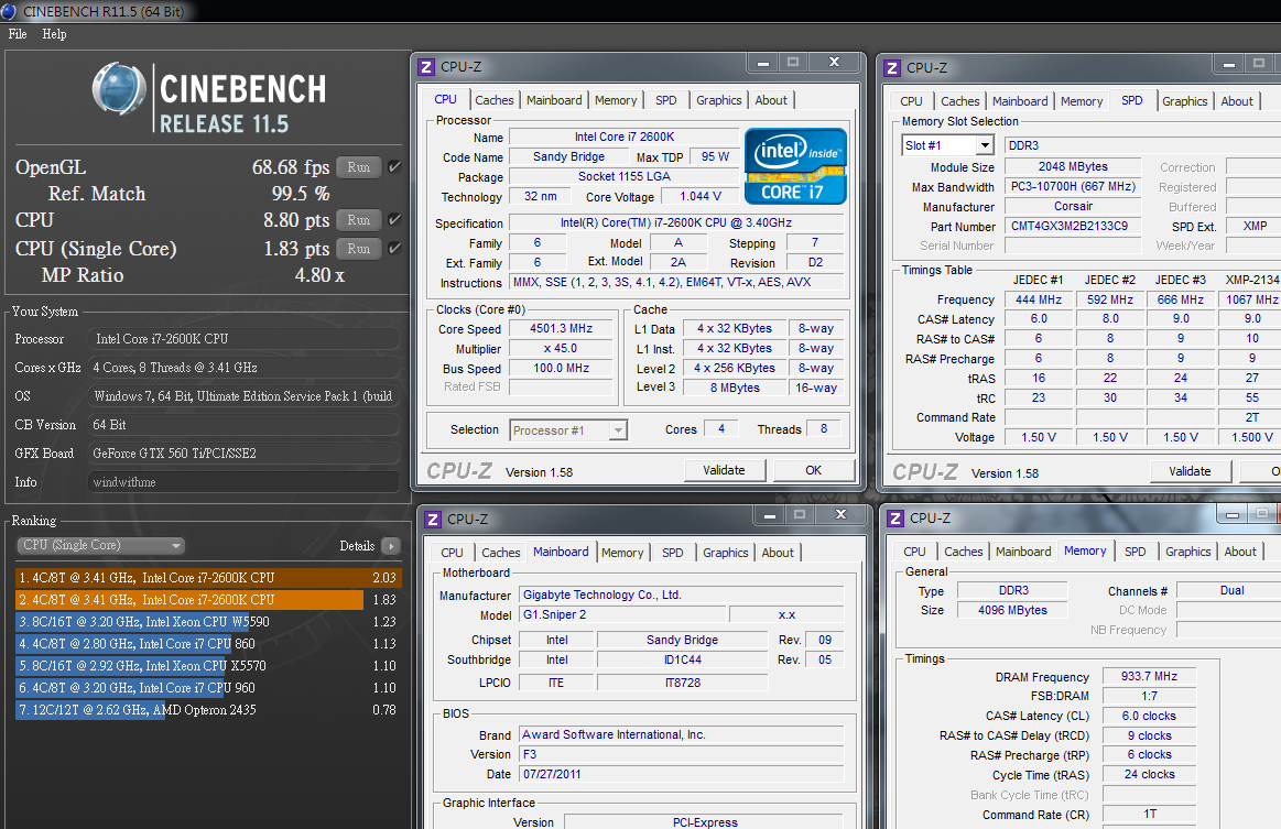
PCMark Vantage => 24328

The CPU voltage will be various as different CPU quality.
Actually, if the cooling is good, 2600K no need to add too much voltage from 1.245V to 4.5GHz.
The above test is setting as 1.250V. It can pass most benchmark software and burning test stabile.
Sandy Bridge as Intel 2nd generation Core I structure. The CPU single thread performance is excellent.
4.5GHz clock to test all benchmark, the score and performance are very good.
Also, OC to 4.5GHz is a stage. You have to control voltage and temperature well.
DDR3 Test
ADIA64 Memory Read - 22282 MB/s
Sandra Memory Bandwidth - 24726 MB/s
MaXXMEM Memory-Copy - 24863 MB/s

Sandy Bridge DDR3 bandwidth improves a lot. It’s even same as LGA 1366 3-channel.
If DDR3 quality is good enough, even CPU clock is the same, you still can run at 2133.
Using CORSAIR DOMINATOR-GT to test 1866 CL6, the bandwidth and performance are very good.
Temperature Test (Room Temperature 28℃)
Enter to OS Desktop - 33~38

CPU Full Speed - 56~64
Intel Burn Test v2.4,Stress Level Maximum
The temperature result is good. It owes to H80 water cooling system as well.
2600K OC to 4.5GHz won’t be a problem if you use mid-high end coolers.
This is also 32nm advantage. I am looking forward to Panther Point next year.
Power Consumption Test
Enter to OS Desktop - 100W
OCCT Power Supply Mode - 410W

For 2600K OC to 4.5GHz add GTX 560 Ti, the power consumption is very low.
For full speed, CPU full speed is around 200W and above test OCCT CPU and VGA is 410W.
This value just needs 550W PSU for whole system.
GIGABYTE hasn’t implemented UEFI interface, but it provides alternative solution called Touch BIOS software.
Users can adjust BIOS items in OS and also support touchscreen LCD.
This software also integrates many GIGABYTE features. It also provide multilingual interface. The screen shot is Traditional Chinese.

BIOS is not UEFI design, but it means user can use BIOS interface in OS?
When I see items called "Miscellaneous Settings", I can imagine how rich the settings are...
-
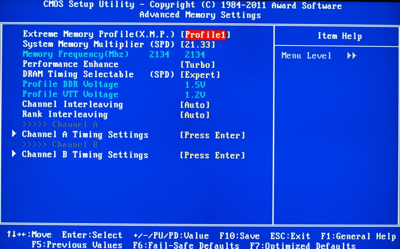
Advanced DDR3 Parameters Setup Page
The screen shows setting as DDR3 2133 CL7 10-7-27 1T

Voltage Page
Milti-Steps Load-Line Disabled/Level 1~Level10
CPU Vcore 0.750~1.700V
QPI/Vtt Voltage 0.860~1.530V
Systrm Agent Voltage 0.715~1.495V
Graphics Core 0.850~1.705V
CPU PLL 1.195~2.435V
DRAM Voltage 0.890~2.135V

Sniper2 built in one HDMI output. User can use for Intel built-in GPU.
It bundles with Lucid Virtu GPU Virtualization technology for user to switch high end 3D graphic card and Intel Quick Sync Video technology.

PC Health Status
UEFI is a very common word recently. It means 3TB support plus GUI.
GIGABYTE all Z68 BIOS support EFI 3TB HDD. For GUI, they still need to catch up.
This review I use Intel Core i7-2600K. As 2600K default performance, windwithme has test end of 2010.
Recently, the other Z68 OC guide can be reference. If you want to refer to the 2600K default performance, you can search my previous article.
The BIOS pics above are 2600K OC 5GHz setup. You may need to fine tune your system voltage and clock due to CPU and DDR3 quality.
Windwithme reviews are taking long time to fine tune for stable OC.
The OC ratio is passing stress burning which is my own requirement.
Maybe it’s just an easy performance pic, it takes me several hours for fine tune the most suitable voltage and CPU clock for stable running.
With DDR3 OC and fine tune parameters, finally, the CPU and DDR3 are all stable at highest performance.
Then I start to lower voltage to find the lowest value. It takes few hours to days.
I think the every MB best OC setup is worthy and really useful for users who are interested in OC.
I also hope the OC will bring the budgeted hardware into highest performance.
System Configuration
CPU: Intel Core i7-2600K
MB: GIGABYTE G1.Sniper2
DRAM: CORSAIR DOMINATOR-GT CMT4GX3M2B2133C9
VGA: msi N560GTX-Ti Twin Frozr II
HD: Intel 510 Series 120GB
POWER: Thermaltake Toughpower Grand 1200W
Cooler: CORSAIR Hydro Series H80
OS: Windows7 Ultimate 64bit

Cooler is CORSAIR latest water cooling product.
Hydro Series has 4 models, H50, H60, H80 and H100 from low to high.
Below is H80 packing. It’s 5 years official warranty. The package is bigger than perviousH70.
All 4 models support all CPU sockets include future LGA2011.
Left hand is the all black radiator. The size is 120mm x 152mm x 27mm.
The shell is also metal delicate which is better than H70. The both sides can install 12cm fans.
The rotation rate can adjust by the button above cooler head.
There are 1300, 2000 and 2500 RPM. The fan airflow is 46~92 CFM and acoustic is 22~39dBA.
Hydro Series H80 advantage is can install in standard ATC chassis. This hydro cooling is very convenient for users.

H80 new design improves the cooler head. The first one, the new mounting bracket is more stable and durable.
The bottom still keeps the big dimension copper. Next is two 4-pin headers for 12cm fans.
Near the cooler head, there are one small 4-pin and one big 4-pin headers. They are for MB or PSU to supply power to cooler motor.

First of all, let’s test 2600K OC 4.5GHz performance. This setup is most ideal OC range for most suers.
CPU 100.0 X 45 => 4501.5MHz 1.250V
DDR3 1867.4 CL6 9-6-24 1T 1.610V
Hyper PI 32M X8 => 13m 40.699s
CPUMARK 99 => 693
Nuclearus Multi Core => 29030
Fritz Chess Benchmark => 35.31/16949

-
One of G1.Sniper2 key features is Killer E2100 LAN chip, called NPU.
It bundles 1GB DDR2 for network traffic control. It can help to offload the network traffic from CPU.
Another function is Game Networking DNA technology.
It offloads gaming data directly to the NPU by bypassing the Windows Network Stack to save time.

The other key feature is Creative Sound Blaster X-Fi audio processor, chipset code is 20K2.
It built in 128MB Memory cache for 20K2. It’s only for high end Creative sound card.
Nichicon MUSE ES(Green) and MW(Yellow) Japanese made audio caps with metal cover which is same as high end sound card design and components.

Next is G1-Killer series special design heat-pipe. The design concept is shooting game, also called Locked and Loaded Heat-pipe.
The part is a big heat sink. The center has 5 green LED which is on as booting up.

The shape is same as magazine. The top is a copper bullet. The heat sink dimension and quality are impressive.

VRM heat sink is similar to barrel.
CPU is 8 phases Driver MOSFETs design for better power efficiency and temperature control.
Booting Screen

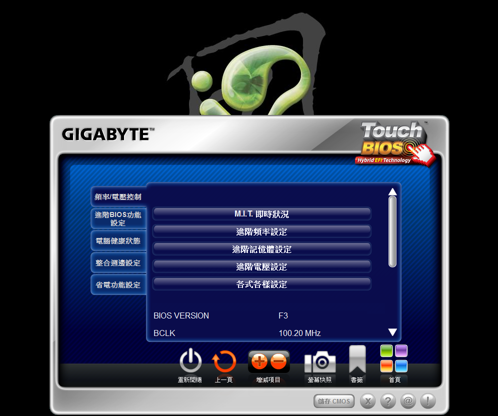
Main BIOS Tuning Menu, called M.I.T.
It shows BIOS version, CPU/DRAM clock, DDR3 capacity, CPU temperature and CPU/DRAM voltage etc.

You can adjust CPU ratio, clock and DDR3 multiplier.
The screen is CPU 100.2Mhz/DDR3 2133 setup.

CPU Detail Items
2600K default ratio is 38, 37, 36 and 35. Turbo Boost 2.0 technology has more critical CPU boost mode.
Internal PLL Voltage Override items enhance CPU stability when OC to 5GHz. Z68 default is Enable.
When OC CPU Clock Ratio to 50, I like to disable Intel Turbo Boost and C1E for better stability.

Memory Setting Page
Sandy Bridge multiplier has 800, 1066, 1333, 1600, 1866 and 2133.
-
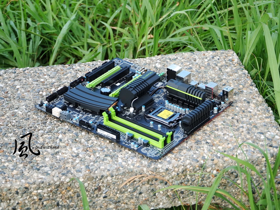
GIGABYTE launched new series in early 2011 called G1-Killer with Intel chipset.
First series use X58 chipset and there are 3 models, G1.Sniper, G1.Guerrilla and G1.Assassin.
They are same as own high end model UD7, but have less power phases and PCI-E slots.
G1 uses high end product components and focus on Gaming which enhance audio and network design.
So far, Intel most popular product is Sandy Bridge.
It’s been launching less than 1 year, however, there are Z68, P67, H67 and H61 chipset can supports SNB CPU.
You can see Sandy Bridge can combine from entry to high end as users demand.
From LGA 1155 CPU and chipset quantity, you can see the product life cycle should be longer than LGA 1156.

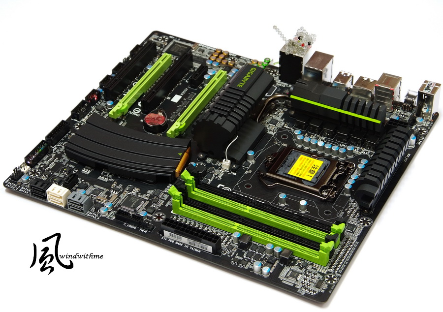
This time, I got GIGABYTE 4th G1 product using Intel latest Z68 chipset with G1 series design concept.
This model name is G1.Sniper2. You can see the color tone is black with green.
It’s same as previous 3 G1 X58 series as focusing on war visual concept.

Sniper2 is ATX and the size is 30.5 cm X 26.4 cm.
It includes 5 Smart Fan controllable fan header which can adjust Z68 platform temperature more efficient.
This time the magazine heat sink has no G1.Killer print. It’s just whole black design.
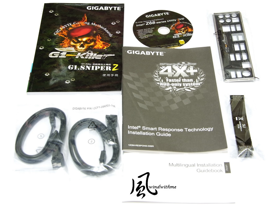
Accessories
Product manual, Software installation guide, Driver CD, IO panel, SATA cables and SLI bridge.
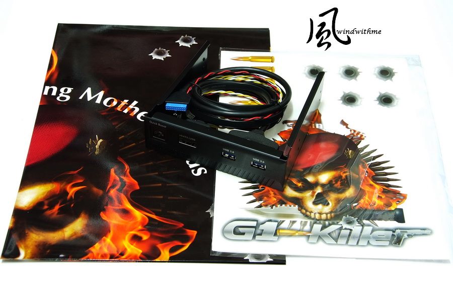
Front Access Control Panel provides 2 USB 3.0 and 1 Power eSATA ports.
Left side Quick Boost button can let user switch to OC mode to increase system performance easily.
Bottom is G1-Killer poster and sticker.
Lower-Left Corner
2 X PCI-E X16 supports AMD CrossFireX/nVIDIA SLI as X8 + X8.
2 X PCI-E X1
2 X PCI
Very rare Bigfoot Killer E2100 LAN Chip.
Built-in Creative CA20K2 audio chip supports Dolby Digital Live, DTS Connect, X-Fi Xtreme Fidelity and EAX Advanced HD 5.0 technology.
It supports max 7.1 channels and High Definition Audio technology.
Design in Taipei

Lower-Right Corner
3 X Black SATA provided by Z68 supporting SATA2.
2 X White SATA provided by Z68 supporting SATA.
You can build hybrid RAID 0, RAID 1, RAID 5 and RAID 10. The max performance depends on SATA devices.
2 X Grey SATA provided by Marvell 9182 supporting SATA3, RAID 0 and RAID 1.
2 X 32 Mbit flash Dual BIOS for dual protection.
Upper-Right Corner
4 X DIMM DDR3 support 800/1066/1333/1600/1866/2133 and DDR3 max capacity is 32GB.
It supports Extreme Memory Profile. DDR3 uses 2 phases PWM and next is 24-PIN power connector.

Upper-Left Corner
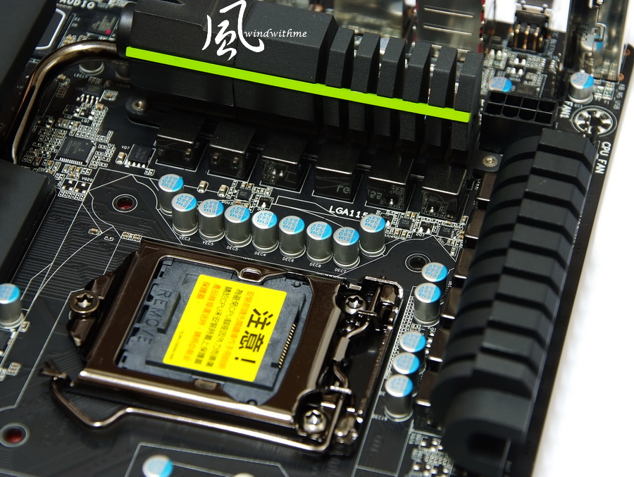
LGA 1155 CPU Socket. The cover is plating process for better quality.
G1.Sipner2 uses 8+2+2 phases PWM. DRAM and Chipset have individual 2 phases.
Behind the upper heat sink is an 8PIN ATX 12V power connector.

IO
1 X PS2 KB/MS
1 X HDMI
1 X O.C. Button
7 X USB 2.0(Red/Black)
2 X USB 3.0(Blue)
1 X eSATA/USB 2.0 Combo(Black)
1 X RJ-45 LAN
1 X S/PDIF optical fiber output
-
BIOSTAR TSERIES TA75A+
PROS
1. The package and material are both above par. The product falls in the mid-price range.
2. The internal display has three kinds of output interfaces, and the 3D performance of the A8-3850 internal display comes close to some basic VGAs.
3. It includes a Japanese solid capacitor, built-in POWER/RESET buttons and a simple debug LED.
4. Its BIOS has been upgraded to UEFI interface, with rich options, a large voltage range, as well as an excellent overclocking capacity.
5. It provides two PCI-E X1/PCIs and integrates the native SATA3 and USB 3.0 technology.
CONS
1. BIOSTAR has no current distribution channel in Taiwan.
2. The DDR3 compatibility could need further enhancement.
Performance ratio ★★★★★★★★☆☆
Material ratio ★★★★★★★★☆☆
Specification ratio ★★★★★★★★★☆
Appearance ratio ★★★★★★★★☆☆
Performance vs. Price ratio ★★★★★★★★★☆
The BIOSTAR TA75A+ costs about US$99(NT$2875) in the U.S.
Its BIOS has been upgraded to UEFI interface, with excellent overclocking capacity and debug LED design.
It has also been integrated with the original new-era specification of the A75 chipset.
It has high competitiveness among the A75 MBs of various brands. However, BIOSTAR still needs to exert effort in terms of increasing its market awareness.
In addition, it should be noted that in CPU overclocking, as the A75 chipset increases the CPU 100MHz overclocking, the SATA frequency also increases accordingly.
If the CPU overclocking is used for a long time, it is not certain whether it will affect the function of the HDD/SSD when operating with increased frequency.
To safely increase the performance of the internal display, the DDR3 frequency should be increased first,
and then adjusted to 1600/1866 to achieve stability according to the physical strength of the DDR3.
The A75 MB with A8-3850/A6-3650 is an all-in-one platform for the mid-range market. It is highly attractive for users who require high specifications.
The major difference with the A55 chipset is the absence of the USB 3.0 and SATA3.
But the product is sold at a lower price and it is definitely a valuable option for entry-level computers.
Specifically, an earlier model of the A6-3500 or a lower-level of the A4/E4 CPU sells for less the price.
When the new-generation APU platform becomes popular in the future, it will be more affordable and valuable.
This is good news to consumers who prefer to purchase low-configuration or entry-level computers.
This article is also post in my own blog WIND3C Welcome your visit.
-
DDR3 1947 CL8 10-8-27 1T
ADIA64 Memory Read - 10971 MB/s
Sandra Memory Bandwidth - 18509 MB/s
MaXXMEM Memory-Copy - 13163 MB/s

Increasing the CPU frequency causes the new FM1 platform to increase the bandwidth for the DDR3 as well.
However, the increased performance is only about 500 MB/s, which is exactly the required enhancement for AMD architecture.
When the overclocking is close to DDR3 1947, it can offer nearly 11000 MB/s bandwidth, which is relatively good for the AMD platform.
The overclocking range of the DDR3 is also increased in the FM1 platform which is normally between 1650-1800 on the AMD platform.
Temperature performance (ambient temperature is about 32 Celsius. )
System standby - 13~16

CPU full speed - 55
Intel Burn Test v2.4,Stress Level Maximum

Test with the AMD C&Q power-saving technology turned on.
The CPU frequency is greatly reduced when the system is on stand-by therefore the temperature is much lower.
When the CPU is at full speed while working with an advanced heat sink, the temperature is acceptable at around 55 Celsius .
I hope that AMD can attain the 32nm process in its CPU series in the future, so as to help increase its competitiveness.
Power consumption test
System standby - 28W

CPU and GPU at full speed - 178W
Power Supply test in OCCT

When the system is on stand-by, power consumption is quite satisfactory due to the power-saving feature.
On the other hand, when at full speed, power consumption is still high.
The 178W-power consumption at full speed is primarily caused by the CPU. This is not good since it adopts a 32nm process.
Compare this with previous tests. The power consumption of Intel’s 32nm CPU at full speed is a dozen watts less than that of the A8-3850.
Power consumption is another aspect that AMD needs to improve on in the future.
It takes a long time to realize the 32nm process, and power consumption could not be reduced effectively.
3D test
Internal display AMD Radeon HD6550D
3DMark Vantage => P5216

StreetFighter IV Benchmark
1280 X 720 => 109.58 FPS

Unigine Heaven Benchmark => 15.3 FPS

In my previous article, I shared the test data of CPU/DDR3 with 100/1866 ratio, and the 3DMark Vantage was about P4500.
This score has reached the same level as the nVIDIA GT430, and it is 10% better than the Radeon HD5570 under the same brand.
In this test, it works with CPU overclocking, so as to increase overall 3D performance by 10~20%.
According to the Llano APU data posted on the internet, the 3DMark Vantage can achieve nearly P7000 at most, which has an amazing 3D internal display performance.
Video Playback Testing
Start up it to play the original copy of a Blu-ray video on hand –named Inception.
Below is the publishing corporation’s copyright ownership.
PowerDVD 10 software
Starting menu
Until now, the CPU occupancy rate is as low as 1-6%.

Playing process
The CPU occupancy rate is 2-10%.

The A8-3850 internal display is represented by the Radeon HD6550D, which is capable of playing 1080P videos.
Generally, the new generation Intel Sandy Bridge and AMD Llano APU have integrated the internal display function to usher in a new era of technology.
Aside from multiplying 3D performance several times, the CPU occupancy rate is much lower than the old platform when playing high-definition videos.
In the future, you need not worry about lagging problems when selecting the internal display platform for playing videos.
-
Performance test
CPU 138.0 X 25 => 3450.3MHz
DDR3 1840.2 CL8 10-8-27 1T
Hyper PI 32M X 4 => 19m 30.146s
CPUMARK 99 => 499

Nuclearus Multi Core => 14018
Fritz Chess Benchmark => 17.77/8530

CrystalMark 2004R3 => 199037

CINEBENCH R11.5
CPU => 4.11 pts
CPU(Single Core) => 1.05 pts

PCMark Vantage => 7420

Windows experiential index - CPU 7.4

Increasing frequency multiplication is a feature not available in the A8-3850.
Also, the external frequency range is not very wide, so the AMD 32nm CPU overclocking limit has yet to be confirmed.
When the black-box edition CPU is released, the overclocking limit of the CPU’s resultant frequency would have a better performance.
According to the above test software, the CPU performance can be increased by 20% after the A8-3850 2.9GHz overclocks to 3.45GHz.
DDR3 is part of the U.S. CORSAIR VENGEANCE series, with model number CMZ8GX3M2A1866C9R
It is indicated on the package that the product supports Intel/AMD platforms, and the DDR3 capacity is 2 X 4GB

The frequency is DDR3 1866, and the parameter is CL9 10-9-24 1.50V
The AMD FM1’s preset DDR3 voltage is 1.50V. Given the preset settings, the DDR3 frequency can be increased to 1866.
If you prefer to just rely on the high-frequency DDR3 and can do without debugging, the DDR3 1866 product is quite good and convenient.
The appearance is also different from the earlier common Dominator design.
VENGEANCE uses the new and large heat sink with elegant red color.

DRAM bandwidth
DDR3 1840.2 CL8 10-8-27 1T
ADIA64 Memory Read - 10555 MB/s
Sandra Memory Bandwidth - 17485 MB/s
MaXXMEM Memory-Copy - 12701 MB/s

DDR3 1866.8 CL8 10-8-27 1T
ADIA64 Memory Read - 9933 MB/s
Sandra Memory Bandwidth - 16127 MB/s
MaXXMEM Memory-Copy - 10979 MB/s

-
The heat sink covers the AMD A75 chipset.
Despite its small volume, the BIOSTAR heat sink appears to have better texture.

The heat sink in the power supply uses eye-catching colors. The design makes heat dissipation conveniently larger.

BIOS home screen

O.N.E. debugging page
The CPU Clock is one of the key points of overclocking. If the HDD/SSD on the SATA device is powerful enough, it could reach 140~155MHz.
The IGD Clock Control adjusts GPU frequency, but increasing the frequency doesn’t help 3D performance.

To start from the Core FID is recommended followed by a reduction of the CPU frequency multiplication and an increase in the external frequency of the CPU;
these would result in a wide overclocking range.

Voltage page
APU-Core Over Voltage +0.050~1.450V
APU-NB Over Voltage +0.050~0.200V
DDR Memory Over Voltage -0.400~+0.450V(BIOS data 1.596V)
APU DDR-PHY/PCI-E Over Voltage +0.010~0.450V
FCH Over Voltage +0.010~0.450V

DRAM parameter settings
The most efficient way to improve the 3D performance of the Llano APU is to increase the frequency of the DDR3.
To increase the external frequency of the CPU, it is recommended to first set the DDR3 at 1066/1333.

More advanced DDR3 parameter options

PC Health Status

So far, the A75 overclocking has two internal display GPU methods.
One is by taking the default CPU value and setting the DDR3 at 1600 or 1866 operation.
The other is by reducing the CPU frequency multiplication and the DDR3 frequency, followed by increasing the CPU external frequency to achieve the main purpose.
The former is a simple and stable overclocking method while the latter is for users who want to explore the CPU/DDR3/GPU performance limits.
The BIOS setting mentioned above applies the latter’s overclocking method.
It took me quite some time to achieve this setting.
Test platform
CPU: AMD A8-3850
MB: BIOSTAR TSERIES TA75A+
DRAM: CORSAIR CMZ8GX3M2A1866C9R
VGA: AMD Radeon HD6550D
HD: WD3200BPVT 320GB
POWER: CORSAIR Builder Series CX430
Cooler: Thermaltake BigTyp 14Pro
OS: Windows7 Ultimate 64bit SP1

-
In early July, AMD released a new platform with FM1 pin grid array, which supports the CPU and adopts an updated APU technology.
It has updated its own architecture and integrated a GPU with higher performance into the CPU.
For users who support the reasonably-priced AMD, this is definitely another option with new specifications.
In 2011, AMD plans to release a CPU with higher performance called the Bulldozer which is set to strengthen its medium and high-end product lines.
The Llano APU platform has two kinds of chipsets, the A75 and A55. The newly released A55 has low configurations.
In the past, the quad-core CPU only had two options, the A8-3850 and A6-3650. However, recently the tri-core A6-3500 was released to the market.
When the A55 gains a foothold in the market in the future, it can combine with the A6-3500 to present a valuable, new generation high performance internal display platform.
I (nickname: windwithme) have discussed the A75 performance of the Micro ATX in my last article, and now I will talk about the A75 MB of the ATX specification.

The greatest feature of the A75 is its capability to provide native support of USB 3.0 and SATA3, as well as a wider range of specifications.
Major MB brands have many A75 models available in the market and hopefully, there would be an A75 product with ITX specification released in the future.
I patronize the BIOSTAR TA75A+. The BIOSTAR brand is affordable and has overclocking features; it represents a relatively good C/P value.
The package adopts a simple design with red color and words/patterns that describe the supported functions and technologies.

Attached accessories
User’s manual, IO board, SATA wires and software driver disc

BIOSTAR TA75A+ appearance
The advantage of the ATX is its good scalability. Its large size makes the computer mainframe larger.
Choosing the A75 of the Micro ATX or ATX specification depends on the different requirements of users.

The PCB is black in color while the other extended slots are either red or white.
I believe that replacing white with black would bring better texture.
Currently, many advanced MB products generally use black and red colors.
This is because black appeals to a lot of consumers.

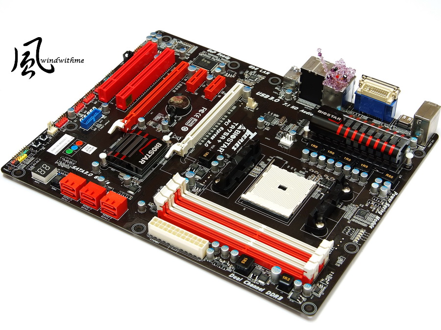
The lower left section of the motherboard
2 X PCI-E 2.0 X16 supports 2Way CrossFireX technology, and the bandwidth is X16+X4
2 X PCI-E X1
2 X PCI
Realtek RTL8111E network chip
Realtek ALC892 audio chip supports 8-channel HD Audio

The lower right section of the motherboard
4 X red SATAII connectors are provided by the A75 chip; these are of SATA3 specification and support RAID 0, RAID 1, and RAID 10.
Blue is the front extended USB 3.0 slot, Power, Reset buttons, and a simple built-in Debug LED

The upper right section of the motherboard
4 X DIMM DDR3 slots support 800/1066/1333/1600/1866/2000(OC), and the highest DDR3 capacity supported is 32GB.
Specification of DDR3 2000 can be only achieved through CPU overclocking, along with a 24-pin ATX power connector.

The upper left section of the motherboard
TA75A+ requires 4+1 phase power supply, supports AMD A8/A6 CPU and A4/E4 series to be released in the future.
The 8-pin power input is positioned in the upper left. In the past, the AM2+/AM3 heat sink were also installed on the FM1 pin grid array.

IO
1 X PS2 keyboard
VGA/DVI/HDMI
4 X USB 2.0(black)
2 X USB 3.0(blue)
1 X RJ-45network hole

High-end NB for Gaming and Movies - MSI GT683R notebook
in General hardware discussion
Posted
Windows7 benchmark
GT683 built in with Core i7-2630QM, the performance almost 2x of i5-2410M which I did share the benchmark in one of my other review last time.
The performance of Core i7 is really excellent on single or multi tasks, also the only Quad Core CPU segment of Intel platform.
Normally Core i7-2630QM is 2GHz, but through TurboBoost 2.0 technology, it will mostly run at 2.4~2.6GHz, this performance level already great enough for a gaming notebook.
SATA performance tests
HDD used WD5000BPKT black label with RAID 0. Format is 2.5” SATA3; seek time 12.0ms, 16MB buffer
HD Tune Pro 4.61 Benchmark
Read - Average 162.0 MB/s Access Time 16.0ms
CrystalDiskMark Seq - 173.3 MB/s Write - 184.3 MB/s
HD Tune Pro 4.61 Benchmark
File Benchmark highest write in speed close to 175MB/s
ATTO DISK Benchmark will reach 197/3MB/s reading speed when over 64k data tests, and writing speed is 200.3MB/s
BootRacer
Time to Logon 18 seconds
Time to Desktop 34 seconds
Because of dual SATA3 design, a great advantage of 15.6” GT683R, normally we only see dual HDD design on 17” or higher size notebooks.
If users what bigger capacities and higher performance at same time, use 2 same capacity HDD become RAID 0 is good solution.
It will make HDD performance up to 2x speed and also with 2x HDD capacities. MSI already built in some software and present fast boot up into Windows7 quickly.
2 SATA3 port is very flexible for HDD or SSD combination, I take over the bottom cover to take a look the inside design.
2 WD HDD is on up left and down right side, only with 2 DIMM slot, guess another 2 DIMM is under keyboard.
Here comes with big size thermal module design for whole system
Used 2 heatpipes for CPU to pass the heat from Intel Core i7 2630QM, nVIDIA GeForce GTX560M used 3 heatpipes to pass the heat.
The MXM VGA card is nVIDIA GeForce GTX560M under the heatsink, if the MXM card comes with same format and size, it seems still have some room for upgrade?
The highest temperature of whole system is GTX560M, after burning test, I use hand to touch CPU heatsink could stay over 5sec,
but to touch the heatsink on GPU I cannot stay over 3sec, temperature always a priority topic from nVIDIA and needs to make some improvement.
The second way to improve the performance is to use 1 SSD become system disk and keep 1 HDD as data disk.
CORSAIR Force GT series support SATA3, with much higher performance than SATA2 SSDs.
Formal data shows this SSD could reach 555MB/s reading speed, 515MB/s of writing speed (Used ATTO DISK Benchmark).
CORSAIR Force GT Series used red shield looks; MTBF is 150k hours, 3 years warranty.
Installed the Force GT SSD into GT683R, this combines greater performance and still keep most capacities.