

digitalbath
-
Posts
96 -
Joined
-
Last visited
-
Days Won
2
Content Type
Profiles
Forums
Events
Blogs
Everything posted by digitalbath
-
A7N8X-E Deluxe as an alternative for socket 462
digitalbath replied to TerraRaptor's topic in Mainboards
I tried also to make a mockup with paint. I am not sure if this is possible. Dividing romsips in two parts maybe helps to get them in the second column? Using two tabs (one for DRAM timings, one for chipset) should be not a problem for me.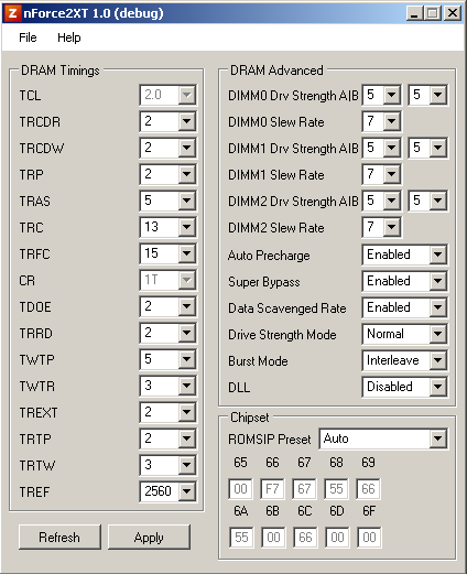
-
A7N8X-E Deluxe as an alternative for socket 462
digitalbath replied to TerraRaptor's topic in Mainboards
@InfraRed Good job! I will use your latest version for my tests. I would like to see two seperate drive strength per dimm (if there is enough room for it). I don't think it will change our overclocking ability that much. But it is nice to have. @Tzk something like this? ? still testing though. I will try get a higher result. -
A7N8X-E Deluxe as an alternative for socket 462
digitalbath replied to TerraRaptor's topic in Mainboards
As far as i see, register 70+71, 74+75, 7C+7D, 99, 9A, 9B and F9 depends on FSB speed an CAS Latency. I have no clue what the values means. Changing one register in 71 / 75 (bit 13 in 70/74) and the system crashes. -
A7N8X-E Deluxe as an alternative for socket 462
digitalbath replied to TerraRaptor's topic in Mainboards
Good luck with that! the post in the nForce tweaker thread says: To change from CAS 2.5 to CAS2.0 you must change this Offsets PCI Bus#0 Dev#0 Func#1 Offset# Offset 71 = 24 to 04 Offset 75 = 24 to 04 Offset 9A = 76 to 65 Offset A0 = 6A to 2A Offset A8 = 6A to 2A Offset B0 = 6A to 2A Offset F9 = 46 to 45 On my delta2 board some values are diffrend. By changing one value my system crashes. delta2 PCI Bus#0 Dev#0 Func#1 Offset# cl2,0 cl2,5 cl3,0 Offset 71 = 04 24 04 Offset 75 = 04 24 04 Offset 9A = 54 65 65 Offset A0 = 2A 2A A2 Offset A8 = 2A 6A 3A Offset B0 = 2A 2A 3A Offset F9 = 44 45 45 -
A7N8X-E Deluxe as an alternative for socket 462
digitalbath replied to TerraRaptor's topic in Mainboards
I will try it on my Delta2 / A7N8X-E to check if it reads the right timings. changing CAS in Windows is impressive! I believe, there is only one possible way to check it: set CAS 3 with Winbond RAM? EDIT: Command Rate seems to work perfect an both board. The other readings are correct. nice to see that my BIOS also works for you. I think the romsips presets help boards that can't clock as high as yours. My AN7N8X-E ends at 260MHz. The board will not clock higher with more voltage or other romsips. The Romsips presets should also help with memory ICs that normally runs poorly on nForce2. -
A7N8X-E Deluxe as an alternative for socket 462
digitalbath replied to TerraRaptor's topic in Mainboards
Nice, to see people still working for that socket a platform! As far as I see, secondary timings, tREF, superbypass, data scavenged rate are fine! I never looked at the primaty timings, but they should be also fine. The second register in b0d0f1 / 94 skips any changes and leaves it at 0. As for the CR and auto precharge value, i didn't find it in the registers on my Delta2 Setup. I noticed, the Value in b0d0f4 Register 90-9F changes permanently. The Values seems to depend on the Vdd Voltage. -
A7N8X-E Deluxe as an alternative for socket 462
digitalbath replied to TerraRaptor's topic in Mainboards
A fantastic job Infrared! The romsips profiles and tweakable romsips register will definitely help us! If you need romsips profiles, you can find my profiles in my latest version of the ISA option rom (A6) Beware! The older version of ISA-option-rom (A4) may have a bug on some boards. I will update all my BIOS versions to the latest version. My Romsips profiles are not yet 100% final. We can definitely improve it, but I've had a good experience with it. A7N8X-E_orom_A6.zip -
A7N8X-E Deluxe as an alternative for socket 462
digitalbath replied to TerraRaptor's topic in Mainboards
69h and 6Fh seem to have the most impact on the performance going from 88h + 88h down to 22h + 22h. I will have to test more, but it will take longer... -
A7N8X-E Deluxe as an alternative for socket 462
digitalbath replied to TerraRaptor's topic in Mainboards
I hope someone can confirm that: edit: i think it will help us to test the romsips -
A7N8X-E Deluxe as an alternative for socket 462
digitalbath replied to TerraRaptor's topic in Mainboards
I also don't think it will help us. The program adds detection for mobile processors and FID detection for the K7 processors. The interesting part is that the patch adds two more modules with the patch. -
A7N8X-E Deluxe as an alternative for socket 462
digitalbath replied to TerraRaptor's topic in Mainboards
I compared the FatumNNM Fosage BIOS with the official EPOX BIOS 4729. The BPLs (3.09) are the same. The blocks after the BPL (starting with the fail-safe Romsips) are identical in most cases. The differences are in the end of the first part. It seems this block belongs to the decompression module. There are also changes in the system BIOS. Most strings have been changed. I don't know yet what exactly was changed. i need more time to figure it out... FatumNNM wrote, he used a tool named BIOS patcher. I downloaded it from rom.by and uploaded it here: http://bierbude.spdns.org:2302/USER UPLOADS/digitalbath/BP_ROM.by/ Here are the options, what this tool does: Rom.by contains more Information on BIOS modding. it's worth a look inside. http://www.rom.by/biosedit.htm I didn't find the Explorer program either -
A7N8X-E Deluxe as an alternative for socket 462
digitalbath replied to TerraRaptor's topic in Mainboards
I found his posts in a russian thread (via google translator). He wrote, he got max fsb 283MHz with his Forsage mod BIOS. I found his BIOS here: http://bierbude.spdns.org:2302/Mod-BIOS und mehr/Epox/8RDA+/ this is the changelog: Bios: Forsage based on 8RDA4729 01/25/2006 Attention: I don’t bear any responsibility for the work of this BIOS !!! List of changes / additions: 1 . CPU Interface Table 133, 166 & 200 MHz FSB: (ROMSIP Modding by FatumNNM): - CPU Interface -> Optimal: max. fsb = 283 MHz (in the 2nd channel on Hynix DT-43). - CPU Interface -> Aggressive: Increased 3D stability & efficiency at c. > 10 and> 10.5 (max. fsb = 283 MHz (in 2 channel on Hynix DT-43). 2. BPL updated to version 3.09 3. Command Per Clock: 1T 4. CPU Disconnect feature patched according to nVidia Tech recommendations 5. Dimm Driving Stregth: 6 6. Slew Rate: 7 7. Alpha Memory Timing: 1-3-3-3-3-3-4 8. Increased stability of 3DMark2001SE & 3D applications at higher FSB frequencies 9. Soft L12-mod for non-modal Tbred, Semptron & Barton 10. All modules responsible for operating at higher FSB frequencies were rewritten by me from scratch. In past bios (Sprinter 0.1), I used the 3D-Fire module (by Hell-Fire), it has now been replaced by my NF2Ultra (by fatumNNM). PS: Since mobile versions of AMD are not widespread in our country, I did not begin to correctly detect them. If this is useful to someone, then let me know and I will add this support. looking at the romsips: They seems to be based on DFI-12-31 / Taipan0.3 ED. But he also wrote about more improvements... -
A7N8X-E Deluxe as an alternative for socket 462
digitalbath replied to TerraRaptor's topic in Mainboards
Nice, to find his fingerprints on several boards -
A7N8X-E Deluxe as an alternative for socket 462
digitalbath replied to TerraRaptor's topic in Mainboards
i just found the mixed values on an Epox 8rda bios from 2003/03/05. It seems, they used them earlier than dfi. The romsips from earlier nForce2 boards (8rda, NF7v1) looks more similar to our modded romsips than the stock romsips from newer boards. EPOX also used more romsips tables like DFI. -
A7N8X-E Deluxe as an alternative for socket 462
digitalbath replied to TerraRaptor's topic in Mainboards
Yes, the failsafe tables can left untouched. I just used them to profe my theory. I found the mixed tables only on DFI boards (Lanparty B, U400S-AL ). I wonder why did they do this... ... and why do their tables differ from others? i hope i can learn more about it through more tests ... -
A7N8X-E Deluxe as an alternative for socket 462
digitalbath replied to TerraRaptor's topic in Mainboards
I did tests at romsips and found the following: In my opinion, the first line in the romsips contain coding for the FSB values. In the end, there are usually these values: 0C0C 1010 1414 1818 What struck me is that there is always a jump by 4 values. These 4 values should always be a jump by 33MHz: 100-133-166-200. One value results in 8.33 MHz. If so, then these values (in hexadecimal) should result in: 01 = 8.33MHz 02 = 16.66MHz 03 = 25.00MHz 04 = 33.33MHz 05 = 41.66MHz 06 = 50.00MHz 07 = 58.33MHz 08 = 66.33MHz 09 = 75.00MHz 0A = 83.33MHz 0B = 91.66MHz 0C = 100.00MHz 0D = 108.33MHz 0E = 116.66MHz 0F = 125.00MHz 10 = 133.33MHz 11 = 141.66MHz 12 = 150.00MHz 13 = 158.33MHz 14 = 166.66MHz 15 = 175.00MHz 16 = 183.33MHz 17 = 191.66MHz 18 = 200.00MHz 19 = 208.33MHz 1A = 216.66MHz ... fits perfectly. Now you just have to test it. I do this by changing the values of the rompsips in the main BIOS after the BPL module. One of these four romsips is responsible for the fail-safe boot. the order is usually: 1414 1414 = 166MHz 0C0C 0C0C = 100MHz 0C0C 0C0C = 100MHz 0C0C 0C0C = 100MHz I changed it to: 1414 1414 = 166MHz 0D0D 0D0D = 108.33MHz 0E0E 0E0E = 116.66MHz 0F0F 0F0F = 125MHz after flashing (winflash): A start with the Ins key pressed: So my theory should be correct. -
A7N8X-E Deluxe as an alternative for socket 462
digitalbath replied to TerraRaptor's topic in Mainboards
I have modded a BIOS for the ASUS A7N8X-E, based on the latest official 1013 BIOS. There are still small points to be improved, but so far it is going well for me and without problems. USE AT YOUR OWN RISK! I TAKE NO RESPONSIBILITY FOR ANY DAMAGE THIS BIOS CAUSES changelog: * BPL version 3.19 * [ED55] romsips from Infrared , many thanks! * Soft L12 Mod * AMD Athlon XP-M name * added tRC; tRFC; tREF; DIMM Drive Strength and DIMM Slew Rate options * CPU Interface optimal / aggressive selectable on manual settings * changed Fullscreen Bitmap 1013_ED55.zip -
A7N8X-E Deluxe as an alternative for socket 462
digitalbath replied to TerraRaptor's topic in Mainboards
I compared 4 diffrent NVMM versions. NVMM 4.31 - 02/24/04 NVMM 4.34 - 03/23/04 NVMM 4.35 - 07/02/04 NVMM 4.40 - 04/29/04 I tested it with modified ED55 romsips from Infrared on my Delta2 board. They work very well on Delta2. Thanks a lot for this. Version 4.31 and 4.34 are very similar and work best when the interface is off. Version 4.35 is the worst, but works better with interface on than 4.31 and 4.34. My best results were achieved with version 4.40. It is similar to 3.19. Both 4.40 and 3.19 work well with interface on. The differences are probably only a few MHz. nvmm434-cpc-on.bpl -
A7N8X-E Deluxe as an alternative for socket 462
digitalbath replied to TerraRaptor's topic in Mainboards
Okay, I have followed your suggestion and overwritten the second block with 0. The board does not boot with 4.85 and 4.08. 4.31 is going well. Performance is comparable to 4.40. Now we have three working versions for the newer boards: 4.31, 4.35 and 4.40 -
A7N8X-E Deluxe as an alternative for socket 462
digitalbath replied to TerraRaptor's topic in Mainboards
I will try the NVMM bpl on my Delta2.The delta2 board needs the 4.xx version for the right RAM auto timing detection. With a 3.xx version the board detects falshe auto timings and therefore does not boot with every ram stick. Manually set timings work without problems. Maybe that's why not every 4.xx version works on the older boards. -
A7N8X-E Deluxe as an alternative for socket 462
digitalbath replied to TerraRaptor's topic in Mainboards
4.62 does not work for me either. 4.40 works on my delta2 so far without problems I think the NVMM bpl was only made for the boards with the southbridge update