-
What's the correct category on hwbot for my APU?
Greetings. A question regarding the embedded Kabini cpus quoted above. This is reported correctly in the HWBot database. For example a GX-415GA has a 8330E gpu (as stated) and there's a 8330E category available. Should i still submit into the 8330 mobile category as stated in the table?
- I.nfraR.ed - NF7 V2.0 @ 306.8MHz - 306.83 MHz Reference Frequency
-
TAGG - SDR SDRAM @ 216.9MHz - 216.9 MHz Memory Frequency
You even found a way to bypass the MUX switch for the SMBus which allows the usage of setfsb. Well done!
- TerraRaptor - SDR SDRAM - 242.5 MHz Memory Frequency
-
Most Miserable Frequency Reached with a Duron
Few thoughts: 1. you can't change multi on-the-fly on NF2 2. lowest multi is either 4 or 5, 3x is not possible. You can read the AMD datasheets for the available multis. iirc lowest is 5x... 3. there's Infrareds NF2 Xtreme tweaker available for NF2, however the lowest it can do is 50MHz. Maybe @I.nfraR.ed can lower that limit, so you can test if you can reach as low as 33Mhz? And at last: nice job, well done!
-
Socket 462 BIOS workshop
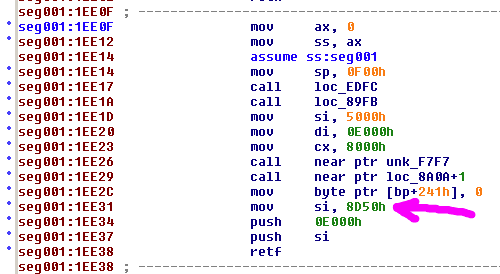
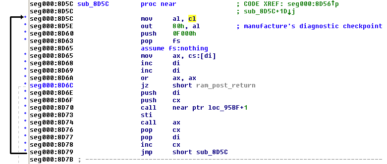
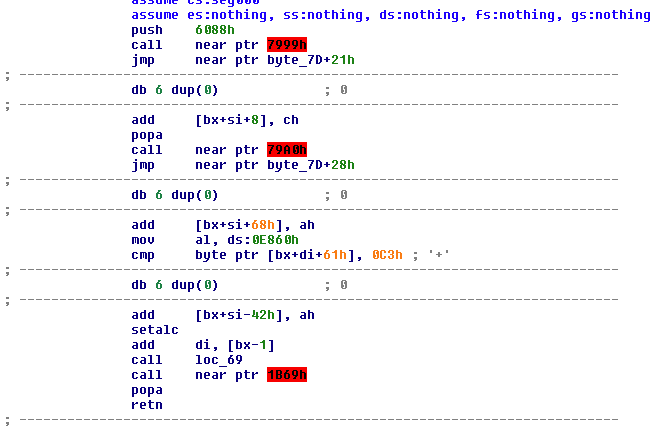
Let's talk about the POST code jump table inside Award v6.0PG Bios. I'll use the Asus A7N8X-E Deluxe 1013 bios as example bios. The POST code jump table is located inside the original.tmp or system.bin inside the bios. So the first step is to extract he system module with cbrom. Afterwards we can load it into the disassembler of our choice. Before we dive into this, please be aware that the system bios is usually 128kb in size and split into two 64kb segments. Usually these are refered to as E and F segment, as this is where they get loaded to when the bios is read and processed by the cpu. As the system.bin is 128gb in size, we get hex offsets from 0h to 20000h. The lower half becomes the E segment, so 0h - 10000h is mapped to E000:0000h - E000:FFFFh and the upper half becomes F000:0000h to F000:FFFFh. Keep that in mind when you stumble across far jumps or the bios loading 0E000h or 0F000h into registers. Usually this means that a far jump to the other segment is about to occur. Luckily Award seems to use the same entry point into the system bios on several bios versions. So in our case we have a look at offset F000:F80Dh (remember, that's stored at 1F80Dh in the system.bin file!) and notice that award stored a jump instruction at that offset. It's a jump to F000:EE0Eh, that might differ on your bios. The interesting part sits down a bit further, the bios moves offset 8D50h into the si register, pushes 0E00h and then returns. We follow that offset and have a look at E000:8D50h. Now, let's have a look at the new offset: We're presented another offset 8D7Ch (that one is actually the first entry in the post code jump table!) and a call to another routine. If all of that fails, then the sytem will jump to HALT. We'll follow the call to E000:8D5Ch for now: This looks like a loop, which iterates through the post code jump table. Nothing to do here, but we found the jump table and we now know how it's accessed. The Post code jump table itself consists of several two byte entries which are pointers to code snippets which prepare the machine for POST, so these initialize controllers, dram, chipset and so on. Some entries are just dummies, so we can make use of this and manipulate either the entry in the table (to point elsewhere) or change the code at the corresponding offset. This allows for manipulation of chipset registers and such, even before the bios initialized it. I believe this is the way to move forward and away from using a ISA or PCI option rom to manipulate chipset registers. ---------- If you want have a deeper look into the topic, read chapter 7.2 here: https://sites.google.com/site/pinczakko/pinczakko-s-guide-to-award-bios-reverse-engineering#Original_tmp
-
PLEASE ADD MOTHERBOARD THREAD:
please add mobo Tyan Tiger MP S2460 Chipset is AMD 760MP (already in database) https://valid.x86.fr/wykzrx https://www.ultimateretro.net/en/motherboards/10578
-
Tzk - A7N8X (rev2.0) @ 289.2MHz - 289.17 MHz Reference Frequency
Sorry, haven't seen your reply till now. This is a special bios i made myself, i'll attach it to this post. Note that it is made for the regular A7N8X Deluxe v2.0, but won't work on the -E Deluxe. I got a special OEM board which is basically a stripped Deluxe, but only has non-deluxe features (hence called "4MBO" on the sticker on the LPT port). Not sure this bios works on regular A7N8X v2.0, you might have to disable "speech output" in bios to get it to boot properly. If you want to try other romsips, take a look here: https://biosbude.de/! BIOS VAULT/Asus/A7N8X Deluxe rev 2.0/digitalbath/ And if you got -E Deluxe, try one of the files ending in B2A from here. I'd try 619XT_B2A first: https://biosbude.de/! BIOS VAULT/Asus/A7N8X-E Deluxe/digitalbath/ A7N8X_20_ED55_B2A.zip
-
Socket 462 BIOS workshop
To expand on this a bit further, i dug deeper through the system module of the 1013 bios. There are several of these pointer tables which reference both, an item string and a bit of assembly code. I noticed that these pointer tables aren't stored at the same place inside the module, but the position varies. Also at offset 12B64h and 12B96h there's two pointer tables stored next to each other. That got me thinking... How does the bios know that the next block of bits is indeed an index, pointer table or whatever else? So i concluded that there must be another lookup table somwhere which stores the positions of these tables. So basically a master lookup table, so the bios knows where to look for the (sub) tables. As x86 cpus and offset usually work in little endian, i decided to convert the offsets of the pointers mentioned earlier into little endian. Also note that we omit the system module offset of 10000h: 12B64h -> 642B 12B96h -> 962B I then searched the system module for these numbers and got a single result (!) for both of them at offset 11B36h and 11B38h. That can't be a coincidence... I haven't analyzed that segment further, but i believe this could be the mentioned lookup table. For further conformation, i will first map out the missing bits of the system module and then try to search for all pointer table index offsets afterwards. Maybe there's more to be found...
-
Socket 462 BIOS workshop
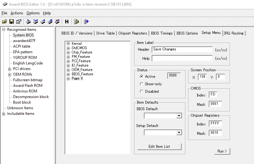
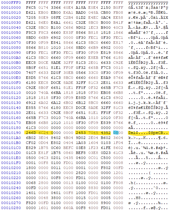
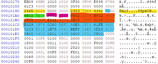
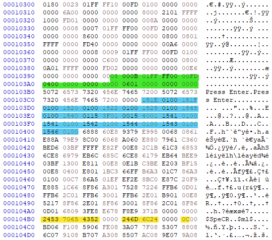
I'd like to document my findings on item string inside the Award 6.00PG bios of my A7N8X-E Deluxe. The version i'll use for this is the latest official, so bios 1013. I guess i mostly figured how the bios items are stored... In Award bios, the selectable items are stored as 25 byte binary strings inside the 128kb system.bin inside the bios file. These strings contain information about the name of the option as link/pointer to the _en_code.bin file (read more about the labels here), where the variable gets stored in CMOS etc. Award groups these strings into pages, just like inside the bios, when the user access it. To gain access to the strings, we need to extract and decompress the system module. We can either do this by using CBROM or AWDBEDIT. We'll for now use the easy way and load the bios in AWDBEDIT. Here's how it looks when we select the System BIOS and then the Setup Menu tab. AWDBEDIT will show all item strings it has found in the list, grouped by pages. We now know that there are 9 groups inside this bios. We'll now extract the system module and open it in our prefered hexeditor, in my case HxD. The hex offset where the strings are stored is 10000h. Here's how this looks. Note the "magic number" which is marked in yellow. There's eight of these magic numbers to be found, so i'll assume that these may indicate the start of a bios page. From the start of the segment at 10000h to the magic number at 10190h seems to be unreadable gibberish, we'll talk about that later. Before that, we'll have a look at the section below the magic number. It seems like some bios item strings got assembly code attached to them, while some don't. The indicator for this is a small lookup table below the magic number and the blue 08h. It indicates that there's eight bios strings in this bios page which got code attached and is followed by a pointer table. That pointer table consists of a pointer to the bios string and a pointer to the code table. Each pointer is 4 bytes long. I marked two of the eight pointers in green and pink. The green pointer "6b02" directs to the item string at 1026Bh (note the little endian notation) and to the code block "3E04" at 1043Eh. The pink block directs to 10284h and 1044Bh respectively. The other six pointers are marked as orange block and work just like the first two. These pointers are then again followed by a block of "gibberish", marked as big blue block. Below that, the actual bios item strings are stored. In this case there are 18 strings. In the following shot, the 18th string is marked in green. It is followed by two text strings "Press Enter". Afterwards there's again some kind of (yet) unknown lookup table, which consists of 16 seven or eight byte long groups. This section will need further investigation. There are followed again by gibberish, but in this case the table with pointers to strings and code from above brings us here. So it's safe to assume that this section is actually assembly and will be executed when the user accesses the corresponding bios option. At the bottom, this code block is followed by the next magic number (marked in yellow), indicating the end of this page and the start of another bios page. ---- That's it for the structure of the bios pages. We now know that these consist of bios strings and code (if nessecary). Now, we'll extract the bits that we called gibberish above and run them through a decompiler. We find that all of this is actually assembly code. Even the block in front of the first magic number is code... So we need to investigate this further to fully understand why Award did this. ------ To close things up for now, i'll attach a textfile where i split the binary data in sections and arranged it into "data" and "code": offsets.txt
-
-
TAGG - Athlon XP 2700+ (Thoroughbred) @ 3132MHz - 33sec 94ms SuperPi - 1M
Great score! I love how the underrated A7N8X is flying lately. Never imagined that it'd become a board which is on par with Abit and DFI about 2 years ago ❤️ And yes, socket 462 is fun. People just seem to have forgotten about it back when 939 hit. 462 ist just right inbetween soldering clock generators to get additional clocks and applying some settings in bios - so perfect for hardcore tweaking ?
-
Links to identify DDR/DDR2/DDR3
DDR1 Twinmos, ending of the P/N: 1GA-T -> UCCC AADT -> Powerchips 5 ns 130 nm CADT -> Powerchips 5 ns 110 nm AADW -> Hynix D43 1AMW -> Hynix D5 A-T -> Powerchips S9DT -> Powerchips 1A4T -> UTT BH-5 1A4B -> UTT BH-5 AA4T -> CH-5 DDR1 GEIL, SN: 1074, 1075, 1256, 1259, 1292, 1243 -> UTT 0746, 0753, 1730 -> TCCD 1746 -> suspected to be TCCD EDIT history: 2023/01/26 add Geil SN 1256 (UTT)
-
Socket 462 BIOS workshop
You were right, the SYSDCIN is indeed a 4 bit register. This is taken from the AMD-762™ System Controller Software/BIOS Design Guide, page 64 (24462.pdf). Note that it says that 0b1111 = 16 clocks is a valid value for this register. I also noticed that there's a lot more SIP registers which the AMD 762 chipset uses. The datasheet also mentiones that the SIP values are sent to the cpu, so these values should be present on all socket 462 chipsets, but maybe stored on a different way. So my suspiction is that the NF2 does also have these stored somewhere. As i also suspect that Nvidia actually licensed the IP of the chipset from AMD, which would make the NF chipset a successor of the AMD 760/762, this might help us a lot with romsips. Remember the Xbox story where Microsoft wanted to use AMD cpu and chipset? The story where a last minute swap to cpus by Intel forced them to rename the chipset, so the chipset wasn't advertised and made as AMD but nvidia? Iirc they even had to build either a intel cpu which could deal with EV6 bus or a chipset to accept the intel bus protocol... Anyways. Here's what i found in the above mentioned datasheet, namely in the B0:D0:F0:60h to 70h register. Note that the datasheet got these tables multiple times in it. I suspect this is because the 762 chipset can handle dual-cpu setups, so you need them for cpu #0 and cpu #1. And there's even more in this pdf... Seems like AMD implemented drive strength and slew rate for the FSB (not dram!) and even more timings.page 43 and 52:
-
Socket 462 BIOS workshop
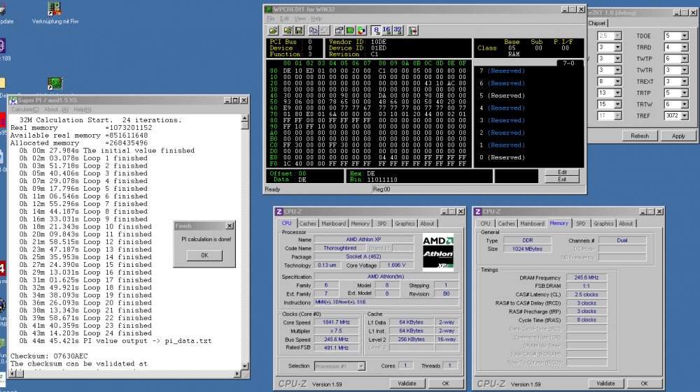
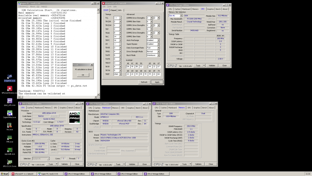
As the Asus A7N8X in particular is very picky when it comes to ram, i'll share what i found when trying to pass 32M at high fsb. The sticks in question are: any TCCD stick, here: Corsair XL v1.2 2x512mb Crucial Ballistix PC3200 2x512mb (Micron 5B-G), Twinmos Twister "new BH-5" 2x512mb (UTT BH-5) First i did several hardmods to the board. These are: recap with polymer capacitors 12V rail mod for cpu lower the resistance of the feedback divider of VDimm VRM VTT mod (not used here) Vdd mod for the chipset I tested the board with Infineon 6A (BH-6) and Hynix BT-D43 256mb sticks first, as these just work on the A7N8X and i'm able to pass 32M up to 263Mhz with them at 1.85V Vdd without much hassle. Without Vdd mod the board won't pass 32M above ~230MHz, so we keep this for all of our tests. I'm also using a bios made by @digitalbath, which got all the new options that we found and developed in the past 2 years inside it. The bios is called ED55 B2A, so it uses the ED55 romsips and got the B2A changes for additional romsips and memory controller inside it. The stock bios of A7N8X only got primary memory timings, Vdimm and fsb/ram clocks integrated. The modbios does give us additional options. We get: ram drive strength, ram slew rate, alpha timings, further romsip tweaks, Trc, Trfc, Tref and 2.9V Vdimm. This is essential to push the above mentioned sticks to new limits. ------------------------- Let's start with the Corsair XL v1.2 2x512mb sticks. With all new settings on default, Cpu Interface on, CL2.5-3-3-8 and 2.7V Vdimm i can't pass 32M above 235MHz. If we change the alpha timings from the stock 2-3-5-3-2-2-4 to a lot looser 5-4-6-3-3-5-6, that gives us some extra clock and we may pass 32M at 240. Now we work our way through the drive strength (stock 4) and slew rate (stock 10) settings and set them to 5 / 10. At last we work our way through the custom romsips settings. On my board Hynix #1 gives me another few Mhz extra, as this settings seems the most stable. So here you go, 32M at 245MHz on A7N8X with 2x512mb TCCD sticks. Note that different sets of TCCD may behave a whole lot different. I got two kits of Corsair XL v1.2 (0538 and 0542) and a kit of Geil Ultra-X. The Asus likes the Geil a lot more and i'm able to pass 32M at 250MHz without such trouble as with the Corsair. Also two Corsair sticks are quite weak and won't pass 32M above 235MHz, no matter which settings i apply. So if you're planning to run TCCD on A7N8X, choose your sticks carefully and test everything yourself. ------------------------- Now, the second set. I got two sets of Crucial Ballistix (Batch CL1115T.XY and CL11161.26). The 61 set seems to scale about 5-10MHz better, so i used it for this test. With stock settings i wasn't able to pass 32M at 210MHz 3-4-4-8 with any Vdimm between 2.5 and 2.85V. The system was able to boot at 200MHz 2.5-2-2 but quite unstable. And again we work our way through the settings. At first, we set the alpha timings to 3-4-5-4-3-4-5, tref to 2560, Trc 14 and Trfc 16. We also tighten the primary timings to 2.5-2-2-6 and drive strength 2, slew rate 6. With these settings and the custom #3 romsip preset we manage to pass 32M at 240Mhz. VTT Offset stays stock, as these sticks become unstable when changing it. Above 240, the sticks still crash, so we loosen Tras from 6 to 8 and voila, 250MHz 2.5-2-2 with 2x512mb Ballistix on A7N8X ? Looks like our newly found registers, tweaks and bios has a huge influence and is very powerful... Also the Vdimm feedback rework seems to help by a huge margin. Nice. ------------------------- Let's move to the last set, namely the Twinmos Twister new BH-5. If you search the web for socket 462 results of these sticks, you mostly get posts of people complaining about incompatibility and all sorts of issues. I own two kits of these and all sticks are able to pass 32M between 250 and 260Mhz at 3.4-3.5V on socket 939 (Ultra-D). However on A7N8X with stock bios they even struggle for stability at 200MHz 2.5-3-3, no matter of VDimm applied. At 183MHz 2-2-2-11-13-15 and 2.8V the system was stable. Interestingly going above 3.2V Vdimm even made things worse. This is quite strange behaviour for UTT BH sticks and i suspect that Twinmos might have not binned those sticks well or the pcb of the sticks (KO-6633) just sucks. The production date on the relabeled chips is 0526 btw. I again started with my ED55 bios and worked my way through the settings. I also tested VTT changes, but deviating from the stock -15mV Offset didn't yield a lot better results. -30mV gave freezes and raising the VTT to 0mV Offset (so exactly 50% of VDimm) made no difference while a positive offset of +30mV made things worse. So i stuck with the stock value of -15mV. I also tested drive strength and found that the range between 4-6 was most stable. Slew rate was kept at the stock 10, as lower or higher settings made things worse. With these settings and alpha timings of 2-3-5-3-2-2-4 i was able to get the sticks stable at 210MHz. A little improvement, but still dissapointing for UTT BH-5 sticks. At this point i decided to call it a day and just put the twinmos back into the drawer. There's no point in wasting more time on these sticks. So no 32M screen here, i just gave up...
-
Tzk - A7N8X (rev2.0) @ 289.2MHz - 289.17 MHz Reference Frequency
Looks like you can push boards which are capable of 250MHz 32M to new heights, when you use the right settings and romsips ? Not sure the board has anything left in it, but this was literally the first (and only) try to achieve such a high fsb. I made use of the Auto Validation Bot which is implemented in the newest release of the (awesome!) nForce2XT tweaker made by @I.nfraR.ed. Great tool and such a timesaver when working my way up through the FSB range.
Tzk
Members
-
Joined
-
Last visited


