I.nfraR.ed
-
Posts
2473 -
Joined
-
Last visited
-
Days Won
36
Content Type
Profiles
Forums
Events
Blogs
Everything posted by I.nfraR.ed
-
Still looking.
-

A7N8X-E Deluxe as an alternative for socket 462
I.nfraR.ed replied to TerraRaptor's topic in Mainboards
Got the menus working yesterday. Will have to test if I can make Command Rate work. If not, will replace it with Auto Precharge. Using CMOS register 75 for Drive Strength and Slew Rate (4 bits each) and register 76 for the rest (2 bits each, so 2 more bits are free from this register). I was thinking that we could sacrifice some of the IDE Channel options that I never seem to touch and reuse these settings for alpha timings. The menus are setup to save the exact value I need for the option rom without using long switches and comparisons. I will only check for "auto". Also, I've verified everything starts from index 0 - the label groups, the label position in the group, the options, so e.g. 12th group would be 0Bh and not 0Ch.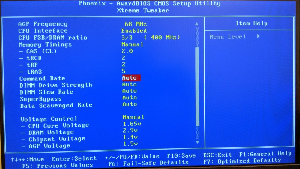

-
So, apparently, we're updating the forum software directly on production, without testing it beforehand? And we don't announce it. There are isp and jQuery not defined javascript errors preventing anyone from posting. Yes, I can post, because I'm a haxx0r, LoL. Edit: Ah, Leeghoofd posted a note in the news section of the site at least, but I still think it was caused by an update.
- 1 reply
-
- 1
-

-
A7N8X-E Deluxe as an alternative for socket 462
I.nfraR.ed replied to TerraRaptor's topic in Mainboards
Btw, I was thinking if it is possible to set Command Rate with the ISA ROM and add that as an option instead of the e.g. Auto Precharge (we have that in windows tools, even without messing with WCPREDIT). That would be more useful, but I'm not sure if it is too late for CR. Would eliminate the need for a separate 1T and 2T bioses. PS: As for the Gigabyte board - all nforce2 boards need mods to unlock the full potential, especially bios. It looks like an OK board, but will have to mod a bios, add missing capacitors, vcore, vdd and vdimm mods. Then it's just a matter of lucky chipset. -
A7N8X-E Deluxe as an alternative for socket 462
I.nfraR.ed replied to TerraRaptor's topic in Mainboards
Yes, that is my point. Moving the Auto to last, so it goes Disabled, Enabled, Auto - 0, 1, 2. Then set default option to 02 and in asm code read register saved settings. Compare to 02 instead of 00 and if not equal, set the actual value to the pci register. You can then reuse the same macro for setting all options with direct value from CMOS and only care about the correct shift, mask and register you want to modify. Congrats once again for the achievement. I think this should be the best bios for the Asus board. And we have the correct PCR files for those who don't have the bios options. If we could find how to add new items then it would be perfect, but works this way, too. Mission accomplished, I would say. Now what is left is to tune for different CPUs, e.g. high FSB and performance versions, 2T bios as well. PS: I can buy a Gigabyte GA-7N400 for like 15 euro and wonder if I should try it. The bios has a lot of hidden options that can be unlocked, but would also need a vcore mod, since it is just +5%, +10%. Same 5 free slots for additional items in bios. -
A7N8X-E Deluxe as an alternative for socket 462
I.nfraR.ed replied to TerraRaptor's topic in Mainboards
Thanks, got it, I think. Abit bioses have 5 free options at the same place. Checked one Gigabyte bios and it's the same there - same 5 options at the same menu. To optimise the asm code, you'd need to move "Auto" to the end of the list and use corresponding Disabled/Enabled or Normal/Fast so they match 0 and 1. For the DS and SR it would work with "Auto" as a first option, since we have the usable options starting from 1 to 15. -
A7N8X-E Deluxe as an alternative for socket 462
I.nfraR.ed replied to TerraRaptor's topic in Mainboards
Ok, so we are counting only heading label, e.g. "Super Bypass" and starting option label, e.g. "Auto". All the rest are managed automatically, thus 5x2 is 10 in total? And you've used the extra 00 bytes just for padding between different heading labels? -
A7N8X-E Deluxe as an alternative for socket 462
I.nfraR.ed replied to TerraRaptor's topic in Mainboards
Alright. Think I got everything that needs to be done, just don't have a way to test it at work. I've been very busy with tasks at work and too tired to grasp the concept easily. It took me a while Btw, it should be possible to optimize all these comparisons of the set value. It should be better to just read the setting, e.g. drivestrength, mask it and set it to the register, instead of doing a switch with 16 cases. PS: Perhaps it's a good idea to put all relevant information from the thread into a new document, so it doesn't get lost so easily. -
A7N8X-E Deluxe as an alternative for socket 462
I.nfraR.ed replied to TerraRaptor's topic in Mainboards
Great work! The asm code is the easiest part for me, since we have a "template" and once everything is in bios, I can write then write the ISA option rom code. I think that I've got how to add the new labels and options and then update the items in "_ITEM.BIN" in the main bios. Will try it when I get back home. You only need to add in _EN_CODE.BIN the starting addresses of the label heading and first option item, right? SuperBypass seems to be enabled by default on NF7, Data Scavenged Rate is also set to Fast. DS and SR are the same for all DIMMs, but DFI sets them differently for the different DIMMs. Will still need to try more combinations, but something like 4/7 and 6/7 works better than the default 3/10. PS: Your code compiles fine under linux. -
I don't know. I only have 3 Ultra-B, one has a blown regulator and I use it for spare parts, the other one has some cut traces to the SB, which could be repaired and it might work again. The working one has the bridging SMD capacitor, others don't. Haven't had a problem with it up to 3.7V VDIMM with just a FB mod. But it's not that great of a clocker compared to one of the dead boards. I hate the Ultra-B layout and don't use it often. CPU capacitors are too close to the socket and get on the way of my waterblock. The I/O ports are also very close to the socket. The 20-pin connector is on the other side of the socket and I need an extension to plug the PSU in. On top of that the CMOS reloaded and loading safe defaults is very unreliable, at least on my board.
-
A7N8X-E Deluxe as an alternative for socket 462
I.nfraR.ed replied to TerraRaptor's topic in Mainboards
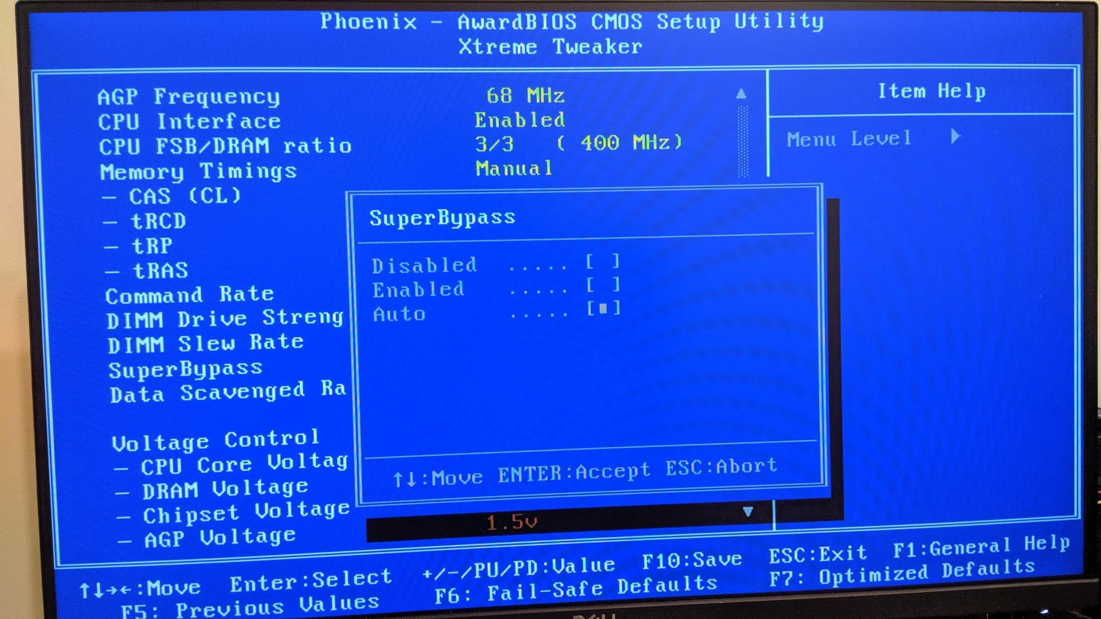
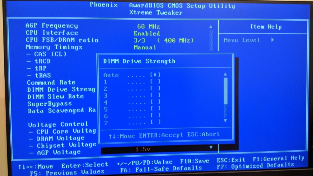
Ok, checked both settings (F8:2)=Data Scavenged Rate 0=Fast 1=Normal (FC:0)=SuperBypass 0=Disabled 1=Enabled b0/d0/f1 Memory Controller 1 Data Scavenged Rate - offset F8, bit 2; 0 is Fast, 1 is Normal SuperBypass - offset FC, bit 0; 0 is Disabled, 1 is Enabled There's one more setting in DFI bios called "Sync Mode Memory Bypass", but the board doesn't boot when set to Disabled. Might be dependant on memory chips or modules installed. Will test more and report back if I find something. Update PCR file attached. Drive Strength and Slew Rate are correct. b0/d0/f4 DIMM1 - DS is 7Ch and 81h, SR is 7Dh DIMM2 - DS is 67h and 73h, SR is 66h DIMM3 - DS is 65h and 71h, SR is 64h Good thing is I can change all of them (DS, SR, SuperBypass, Data Scavenged Rate) in wpcredit on the fly. 10DE01EB.pcr -
A7N8X-E Deluxe as an alternative for socket 462
I.nfraR.ed replied to TerraRaptor's topic in Mainboards
Superbypass seems to be b0/d0/f1 offset FC lowest bit. FC:0 (0000000x) 0 - disabled, 1 - enabled Will do more tests on the dfi, but drive strenghts and slew rates seem to be right. b0/d0/f4 row 90 seems to be changing constantly (autorefresh of rweverything shows that), so 91h is indeed incorrect. -
A7N8X-E Deluxe as an alternative for socket 462
I.nfraR.ed replied to TerraRaptor's topic in Mainboards
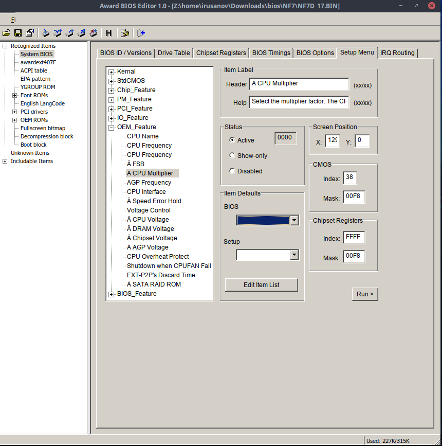
I don't know if it is possible at all, but one possible way is to somehow add a new module with all the subitems and just use an unused label that points to it and opens a subpage (a.k.a [Press Enter]) - basically a mini bios in the bios. Award bios editor has the option to add a BIOS Setup Menu. But I don't know how to make such a menu. On a side note, if you want to change the build date and version number of the modded bios file, edit the system bios with hexeditor - search for the date displayed in cpuz. You can find it on 2 places, e.g. the full date 11/11/2004 and the short date 11/11/04. The version number is taken from one of the bios message strings displayed in award bios editor (second one). It seems to split the string with "-" as a delimiter, so last chars will be the version. Then use the cbrom method to compile the bios back. -
A7N8X-E Deluxe as an alternative for socket 462
I.nfraR.ed replied to TerraRaptor's topic in Mainboards
Thanks for the explanation, I found how to read the cmos regiser in the pdf you linked before. So I now have the idea how to do it. As for the settings, sometimes you'd want different values for different DIMMs I guess, but we can work with same set of settings for now. Don't know if they are the same as on NF4 or from 1 to 8. I also have just 5 free slots in NF7 bios. NF7 sets drv strength at 3 and slew rate at 10 (33/AA) for all dimms at 200+. BPL 3.19 if that matters. Stock is 3.02. It seems you can add labels at the end of _EN_CODE.BIN, but the question is how to add a brand new submenu with as many items as we want. This might require correcting all pointers of the existing items -
A7N8X-E Deluxe as an alternative for socket 462
I.nfraR.ed replied to TerraRaptor's topic in Mainboards
I only miss how to read cmos registers value, but haven't tried anything about it yet. The problem is we have 3 drive strengths and 3 slew rates - 2 settings for each DIMM. Then alpha timings, superbypass, scavenged rate. Did you find how to add more items? PS: Do you read actual bios value or you set your custom default option for the new items? If not possible, maybe set to "auto" and when ISA custom code reads it's not set manually then don't alter it. -
A7N8X-E Deluxe as an alternative for socket 462
I.nfraR.ed replied to TerraRaptor's topic in Mainboards
I have found another version of Award bios editor that shows menu items text (almost) correctly. I don't think it will work for editing, but at least could be used for easier viewing. http://bios.rom.by/ROMutils/Award/awdbedit/re1_25.zip On NF7 I only have 5 unused items, I think. So same as on your Asus.
-
A7N8X-E Deluxe as an alternative for socket 462
I.nfraR.ed replied to TerraRaptor's topic in Mainboards
Got the Nano Flasher too. Tired of the old Willem programmer that requires LPT port, configuration and external power. This should be much easier to work with. PS: By the way, does anyone know how to change the colors of the bios? The modbin option doesn't work, I think it worked for Award 4.xx, but not for 6.00 and I don't know where the colors are hardcoded. -
A7N8X-E Deluxe as an alternative for socket 462
I.nfraR.ed replied to TerraRaptor's topic in Mainboards
Added the known timings in DRAM Controller 1 (B0D0F1). Most are straightforward, except TRAS is controlled with 2 registers. 91:7 controls lowest bit (e.g. 1111 for 15T), while the rest are controlled by 92[2:0]. Also there's not enough space to list all the options for TRFC (32 in total), so I've written just first and last. Will make B0D0F4 (slew rates, drive strengths and the rest) later, but I will probably need to switch to DFI to test them properly by setting them in bios. Also have a PCR file for the Host Bridge by Áedán, but I'm not sure if it is right (10DE01E0). PCR(PCI Configration Registers) Editor / WPCREDIT for WIN32 Copyright (c) 1998 H.Oda! [COMMENT]=Author: I.nfraR.ed, v.1 [MODEL]=nForce2 [VID]=10DE:nVidia [DID]=01EB:Memory Controller (00)=Vendor Identification (01)=Vendor Identification (02)=Device Identification (03)=Device Identification (86:1)=Auto Precharge (90:3)=TRC (90:2)=0000=0T 0001=1T 0010=2T 0011=3T 0100=4T 0101=5T (90:1)=0110=6T 0111=7T 1000=8T 1001=9T 1010=10T (90:0)=1011=11T 1100=12T 1101=13T 1110=14T 1111=15T (91:4..0)=TRFC 00000=0 ... 11111=31 (91:7)=TRAS = TRAS+1 (92:2)=TRAS 000=0T 001=2T 010=4T (92:1)=011=6T 100=8T 101=10T (92:0)=110=12T 111=14T + (91:7) (92:6)=TRCD-R 000=0T 001=1T (92:5)=010=2T 011=3T 100=4T (92:4)=101=5T 110=6T 111=7T (93:6)=TRP 000=0T 001=1T (93:5)=010=2T 011=3T 100=4T (93:4)=101=5T 110=6T 111=7T (93:2)=TRCD-W 000=0T 001=1T (93:1)=010=2T 011=3T 100=4T (93:0)=101=5T 110=6T 111=7T (94:6)=TRTW 000=0T 001=1T (94:5)=010=2T 011=3T 100=4T (94:4)=101=5T 110=6T 111=7T (95:5)=TREXT 00=0T 01=1T (95:4)=10=2T 11=3T (95:2)=TRTP 000=0T 001=1T (95:1)=010=2T 011=3T 100=4T (95:0)=101=5T 110=6T 111=7T (96:6)=TWTP 000=0T 001=1T (96:5)=010=2T 011=3T 100=4T (96:4)=101=5T 110=6T 111=7T (96:2)=TWTR 000=0T 001=1T (96:1)=010=2T 011=3T 100=4T (96:0)=101=5T 110=6T 111=7T (97:6)=TDOE 000=0T 001=1T (97:5)=010=2T 011=3T 100=4T (97:4)=101=5T 110=6T 111=7T (97:2)=TRRD 000=0T 001=1T (97:1)=010=2T 011=3T 100=4T (97:0)=101=5T 110=6T 111=7T 10DE01EB.pcr 10DE01E0.pcr -
It seems to be the same as C7G1 capacitor on the left. Based on the size it should be 0805. I don't know how to get the capacitance without desoldering and measuring. My guess is about 10-47uF, but not sure. Don't have a deep electrical knowledge.
-
I fact this seems to be a factory thing, perhaps some later boards come like that. I think your problem is something else. IMO the Ultra-B is a lot more problematic with bios, although it is the best clocking board out of the box. My 2 older boards don't have this, but they are dead Here's the same on my board: PS: Also my older board without this bridging SMD capacitor (between the mosfets) blew up with a VDIMM mod. I think they added it later to "fix" it.
-
I don't think that black stuff is molten plastic. It looks like some sort of hot glue that someone put on top of these smd elements. The SMD elements you uncovered seem to be fine. Do you have another bios chip to test?
-
A7N8X-E Deluxe as an alternative for socket 462
I.nfraR.ed replied to TerraRaptor's topic in Mainboards
I've already checked 1/21 and 12/31 - they are almost the same and the resulting FSB is the same. It might be +/- 1MHz, but they both load windows at 270MHz and also still unstable at that frequency. Perhaps it's just my chipset limit. Even with slacker memory timings and single channel BH-5 it can't go much higher. I may have found which byte has the greatest impact on FSB, but will do more tests and then share. At least for me, bandwidth numbers don't change, only maximum bootable FSB changes. Even with a stock 133 table bandwidth at 200MHz FSB is still similar/the same. Memory registers are fairly simple to get. I will make a PCR file with all of them + slew rate and drive strengths. Timings are B0/D0/F0, offsets 90 to 97.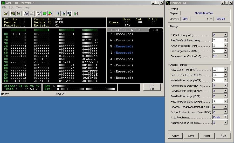
-
A7N8X-E Deluxe as an alternative for socket 462
I.nfraR.ed replied to TerraRaptor's topic in Mainboards
Merlin had been better for me before I made mine, which is very similar anyway. Slew rate and drive strengths can be modified with wpcredit, so I was thinking of using ISA rom to only set SuperBypass and DataScavenged Rate as a starting point. The thing is those registers show different on the NF7 and I'm not 100% sure which bits need to be changed in the whole byte. Will have to test with the DFI board in order to get a better understanding. As for the NF2 Tweaker I can easily make a new similar app to control all timings, since we know the registers already. And there's a openlibsys to help with MSR and PCI read/write operations. I can use the ZenStates app as a base. On a side note, I got 15 sticks of DDR (11 on this picture), but not a single one is Winbond. One of the 2x512 OCZ PC4000 Gold Rev2 (should be Hynix) actually play very nicely on NF2 with default 2.5-3-3-8 1T, but that's not what I'm searching for. Was able to boot 265MHz. Also got the MSI KT880 Delta-FSR, which seems in very good condition, except the CPU VRM capactors, which are bulged and need replacing. Way better built than the Asrock board. -
A7N8X-E Deluxe as an alternative for socket 462
I.nfraR.ed replied to TerraRaptor's topic in Mainboards
I've seen that code and it is quite easy to understand and modify. We can modify it to support all known timings (and other things) for nforce2, however we can already control most of them with windows tools (memset, nf2 tweaker, wpcrset). Worth trying super bypass and data scavenged rate though. Is there a known Tref for nforce2? On the romsip topic - try with one really tight upper half (some 133 table) and see if your FSB drops dramatically as well. Based on this research, I believe native 200MHz CPUs would work good even with stock roms (unless the multiplier table is completely broken). Back in the days those 200MHz locked CPUs were rather limited in frequency by the high multi x 200 FSB combination. And there are just a few 200MHz models. It was all about 133 and 166MHz cpus. I have tried to change some of the bytes in a table, but it was not booting. e.g. (using @TerraRaptor's screenshot) Changing byte 12h to 49 or 89 was no POST, 61 and 69 works (have seen both in tables). The problem is we don't know what are these. PS: Ah, CPU Interface doesn't seem to work on NF7 bios, it always loads the "Disabled" table. That's why I never saw a difference between them - same performance, same max FSB. Have to try if it is broken after the bios menu rearrangement, though. Will have to test with a stock bios. -
A7N8X-E Deluxe as an alternative for socket 462
I.nfraR.ed replied to TerraRaptor's topic in Mainboards
More on the ROMSIP. Testing with XP-M 2500+ and x6 multi. Usual ED multiplier tables, it appears the 133MHz (CPU Interface ON) is loaded. So far, so good. Loads Windows at ~270MHz and goes half way through Pi 1M, but almost impossible to finish it without error. That's what I was experiencing and what I expect. Changing the top part of the particual table with the same part from stock 133MHz table makes the board a little faster, but also drops the maximum FSB to about 240MHz. It seems this is the key for high FSB and that's why modded bioses work - they use the 200MHz table for all. Based on these tests, I think we need to: - Make one "performance" bios with tighter tables for CPUs that are benched at lower FSB and another bios for high FSB, basically 200MHz table copied to 166 and 133 tables (most of the modbioses) - Try to slacken the first part further to allow higher FSB, even with small performance loss (still should be better for super-locked low-multi CPUs). Good for validations, too - Maybe even combine both in one bios, e.g. use the high FSB tables for CPU interface on or off and the performance tables for the other one. Have to check if the difference between CPU Interface ON/OFF is just the tables or it affects the performance in other ways too. PS: That's why L12 hard mod worked as well - making the CPU detect as 200MHz default FSB, so the bios loads 200MHz table, which then allows higher FSB.