
I.nfraR.ed
-
Posts
2473 -
Joined
-
Last visited
-
Days Won
36
Content Type
Profiles
Forums
Events
Blogs
Everything posted by I.nfraR.ed
-
The goal is to support as many as possible. Castle Peak share the same CPUID as Matisse, so it should use Matisse's settings and be detected as such. Currently Matisse, Castle Peak and Rome are set to use the same addresses (in the Debug Tool). Colfax (TR2) is using the same addresses ad Pinnacle Ridge and Whitehaven (TR) - Summit Ridge. PS: I'd be glad if you can run a quick report on one of the 39x0 Threadrippers. Won't find many people using them yet, but want to confirm the addresses.
-
Thanks, we have the 3rd gen Ryzen (desktop) pretty much confirmed. At least with what everyone is running (newer AGESA). It's a safe bet that noone will run really old bios with old AGESA for these anymore.
-
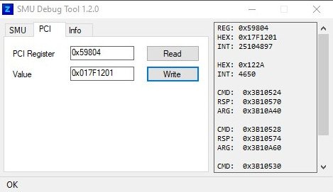
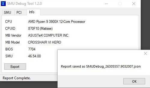
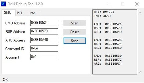
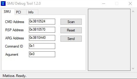
Not being able to get all the missing bits needed to fix the ZenStates app for all supported CPUs I've developed a debug tool to help me test them easier. It started as an internal tool, but grew up and is now available to the public, hoping that it will help me understand things better. TL;DR - Skip to How Can You Help Semi-technical Info Ryzen uses the so-called SMN Mailboxes. As I understand it is a bit of an extension of the standard PCI communication protocol. Basically using special registers/ports for index/data and a set of custom commands for communicating with the SMU (System Management Unit). There are 2 types of commands - "read" which doesn't require a parameter and "write" which sets certain parameter by sending a value to the SMU with the corresponding command. ZenStates and SMUDebugTool use OpenLibSys and WinRing driver for the PCI read/write operations and wraps the SMU read/write around them. There are 3 addresses (+ a pair of standard PCI index/data ports): - MSG Address: Where the Command ID is sent to - RSP Address: Holds the status of the function execution - ARG Address (+5 more, but only one is used): Read the result of a function or where you send the parameter value if the command is of type "write" The workflow for sending a command is as follows: The RSP register is first reset (set to 0), the argument is written to the ARG address and at last the command ID is sent to the MSG address. To check for successful execution you poll the RSP address until a status is returned (0x1 for success, but there are other status coded). If succeeded, you can now read back the ARG address which holds the result. Problem The biggest problem is there's no public documentation for this. Different generations have different addresses and/or commands. SMU version, socket type and CPUID also matter. Throw an ES CPU in the mix and things get even uglier. What I see is AMD kind of unified the 3rd generation and they are more similar than different, but older gens are all over the place. The other problem is to find which commands (IDs) are supported and what their function is. More about the tool It's all manual. The tool detects CPUID and based on that preloads a set of addresses that I *think* would work. It has 3 tabs for now - SMU, PCI and Info. Will add MSR later. 1. SMU Used to test the workflow described above. [Reset] button loads the default set (detected on startup). Scan attempts to find usable mailboxes, which then can be tested with the textboxes on the left and [Send] button. 0x1 command is "Test Message", 0x2 is "Get SMU version". Both are perfectly safe and are the only ones that are always the same for all generations. On the sample screenshot I've first clicked on [Scan] button and then sent 0x6E which for Matisse is returning the maximum (fused) boost frequency. 2. PCI This is no more than a wrapper using the standard PCI write/read. The PCI register is read with [Read] button and the value then displayed in the second field. [Write] button obviously does the opposite - writes the value/config back to the register. On the screenshot I've read the PROCHOT status. This (PCI read/write) can be used on all systems, not just on Ryzen. MSR will be cross-platform as well. 3. Info Displays a basic system info. I'm most interested in the [Export] button. It generates a JSON file, containing the displayed information and also runs the SMU scanner to add the addresses. The file is saved in the same directory where the tool is. A report from my system looks like this: { "CpuId": "870F10", "CpuName": "AMD Ryzen 9 3900X 12-Core Processor", "MbVendor": "ASUSTeK COMPUTER INC.", "MbName": "CROSSHAIR VI HERO", "BiosVersion": "7704", "SmuVersion": "46.54.00", "Mailboxes": [ { "MsgAddress": "0x03B10524", "RspAddress": "0x03B10570", "ArgAddress": "0x03B10A40" }, { "MsgAddress": "0x03B10528", "RspAddress": "0x03B10574", "ArgAddress": "0x03B10A60" }, { "MsgAddress": "0x03B10530", "RspAddress": "0x03B1057C", "ArgAddress": "0x03B109C4" } ] } How Can You Help - Download the app from my github: https://github.com/irusanov/SMUDebugTool/releases - Extract and run it (might need elevated privileges - "Run as admin" if you get WinRing initialization error) - Click the [Export] button in Info tab and share the output here (or where deemed appropriate) Although it seems to be running without issues, I have one report that the scan feature causes BSOD on one Epyc ES, so be aware there's such possibility. As always, I'm not responsible for any induced damage, you run it entirely on your own risk ? It seems ZenStates is not that interesting to the community, but I'd be glad if more people participate, so I can collect more data for different systems and CPU generations. Thanks in advance!
-
 Bad , bad Leeghoofd! You killed the child in me ?
 -
Great one. This makes me wonder if Ryzen + XP + 3DMark 05/06 will be any good.
-
I don't want to justify his actions, but this case I feel is mostly "don't kill the messenger" rather than bashing him for lack of a sportsmanship. If it was not him, there would be others. In some way it is better that it popped up so early in the year. Maybe that was his goal, I don't know. Moreover, Alby wrote that this was a known issue, which the staff hoped(?) won't be exploited. This makes things a lot harder for "Magical USB" guys, but maybe we will now see what they are holding as backups, which is a positive thing
-
TAGG - Sempron 150 @ 6452MHz - 3336 points Geekbench3 - Multi Core
I.nfraR.ed replied to cnzdrn's topic in Result Discussions
Yes, sure. But generally speaking, you need very high CPU frequency to match the score of a DDR3 system. https://hwbot.org/submission/2232551_i.nfrar.ed_superpi___1m_sempron_145_14sec_219ms -
Not to be the bad guy, and I could possibly be wrong, so excuse me if so. But, did you buy 9900K, 3900X, 3960X, 3970X, boards for them and many more Xeon CPUs or do you just use your clients' machines before they take them? Or you bin expensive CPUs to fulfill your clients' needs? How is this exactly fair to other Enthusiast or even Extreme overclockers who buy their hardware on retail prices from the stores? Excuse me if my assumptions is wrong, but everyone visiting your profile can come to the same conclusion.
-
You know that the score will be removed sooner or later, because it is done on Win8 without BenchMate, right? https://hwbot.org/news/9946_application_94_rules/
-
I don't think he has retired, plus he's still active on forums ?
-
A7N8X-E Deluxe as an alternative for socket 462
I.nfraR.ed replied to TerraRaptor's topic in Mainboards
Sorry for the delay, guys. Had a lot to do at work and was too tired. Haven't turned the s.A system on since last time I wrote in the thread. Have some free time at work now, so I will try to briefly explain about the key-in menu. Let's take an example item. The typical item looks like this (25 bytes): 00 00 00 0B FF FF 1F 00 75 1F 00 01 0B 00 00 1F 00 E1 01 00 00 00 00 00 00 According to the info I've shared earlier, first 2 bytes are status. First byte is visibility, second byte is type/function. To convert an item to key-in, I've found that you need to set the second byte to 0B. According to the info, it should be 0x0100 (or 00 10, because it is little endian order), but it didn't work. 0Bh was mentioned in polygon's PDF and it worked. Next 2 bytes are label index and label group index. In my example we have 00 (first label) in 0B (12th group in _EN_CODE.BIN). We leave it untouched. Next is chipset reg and mask, for a regular custom item, chipset reg (04h,05h) is always FF FF. Some of the stock items have them set to point to the actual chipset register. 06h, 07h is Chipset mask. All the documents say it needs to be the same as CMOS Mask. Haven't tried if it is actually the case. 08h is CMOS reg, 09,0A is the CMOS mask. 0Bh is the index to the first label for the item menu and 0Ch is the label group. In this case we set both to 00. I think they are ignored anyway, but we don't need them 0Dh, 0Eh is itemMin 0Fh, 10h is itemMax If we want to support values from e.g. 1 to 15 (1h to Fh), we change these to 01 00 0F 00. 11h, 12h is position on the screen. The modified item would be 00 0B 00 0B FF FF 1F 00 75 1F 00 00 00 01 00 1F 00 E1 01 00 00 00 00 00 00 Keep in mind I write this from memory without actually trying it atm. Hopefully the offsets are correct, but you can experiment.
-
A7N8X-E Deluxe as an alternative for socket 462
I.nfraR.ed replied to TerraRaptor's topic in Mainboards
It's me again Key-in for the FSB frequency. It is supposed to be in DEC, but it appears to be using something like index or whatever. It's not in HEX either. Will play a bit with it to see if I can make it completely working. Maybe use DFI Ultra-D bios as an example or the "Delay IDE Initial" in NF7 bios. Don't have more time before work though. PS: Unfortunately it appears they have used some sort of mapped values, since 187 entries cover the whole range from 100 to 300 and it skips some of the frequencies. Transforming it into a key-in option still uses that table and it is in fact an index and not a direct value. Don't think I will be able to change that, but at least the technique can be used with other (custom) options, where the value saved in cmos register is the same value used for the actual "timing". For example, tREF would have the same issue as the FSB, but those which don't use a key-value map could be transformed. Not that I see any benefit, except you won't need the menu item labels. You loose the "auto" option, so you either allow the user to input 0 (will be treated as auto in the ISA ROM code) or limit the minimum to 1, which then doesn't allow an "auto" option. Not really user-friendly. Initially I thought that it might be possible to somehow shift it from 0-255 to 100-355, but in theory 255 (as a direct value) should be the maximum possible (FF in the register). Won't happen without additional logic in the bios - basically take the exact value and add 100. Not really usable in ISA option ROM, because it is too late. Has to happen much earlier before POST. Wonder if it will work for AGP frequency though. Guess I will be back to ROMSIP testing, but will share what I did for the key-in method later, so we have it documented.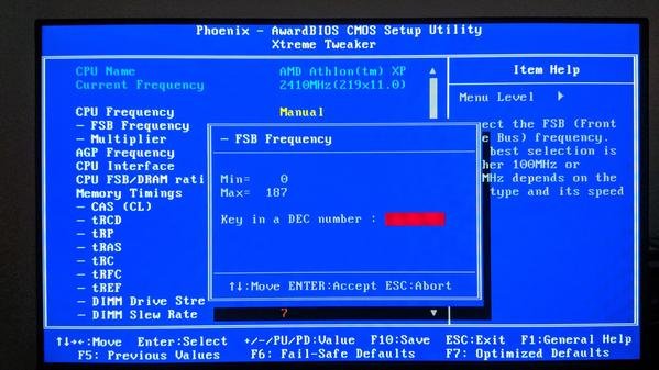
-
A7N8X-E Deluxe as an alternative for socket 462
I.nfraR.ed replied to TerraRaptor's topic in Mainboards
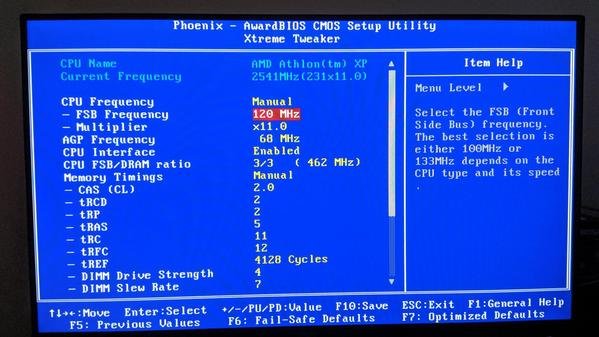
I've tested some values, but don't have more time today. Got some strange results. AA is faster, but also limits the maximum bootable FSB frequency. Difference in AIDA is negligible. Tests done at 11x220, all manual timings. Maybe need to test more values. Trying to run 1M at 260MHz resulted in a lockup. Haven't tried higher Vdimm though. 270MHz is pretty much the limit on this board with BH-5 DC and haven't managed to overcome it. It's not stable at 270MHz. It would be a lucky run if 1M finishes all loops. Pi 4M AIDA FSB 55 03m 25.415s 3459/3463/3449/65.5 270 MHz 22 03m 24.824s 3460/3462/3451/65.3 270 MHz AA 03m 23.923s 3460/3462/3450/65.3 260 MHz Also tried 00 and it was somewhere between 22 and 55, perhaps it is something like "auto". I've also seen DD, FA and FF in 133/166 stock tables. -
A7N8X-E Deluxe as an alternative for socket 462
I.nfraR.ed replied to TerraRaptor's topic in Mainboards
My table is based on one of the 200MHz DFI tables. There are several such tables and they differ in this byte only (if we ignore the multiplier table). One strange thing - initial NF7 bios doesn't have this first part of the tables... -
A7N8X-E Deluxe as an alternative for socket 462
I.nfraR.ed replied to TerraRaptor's topic in Mainboards
It's not really custom, it's from DFI. I've started to play with values and noticed one particular byte changes and it seems to have some effect on stability, but might also hurt performance. Going down to 22 improves stability at speeds close to my maximum 270MHz FSB. I've left it at 55 for now, until I do more tests. This one is also a direct value and can be seen/changed in wpcredit. I think it is b0/d0/f3 around offset 68, but don't have a running system right now to check. The thing that helped most seems to be drive strength and slew rate. 4/7 works better than default 3/10. PS: As for ROMSIP tables, first line changes are only 0Ch, 0Dh, 0Eh, 0Fh. Didn't see a difference between 0C 10 14 14 and 18 18 18 18. Ultimately, I think we can make one bios for TCCD, one for BH-5 (or maybe SR/DR memory) and one for lower FSB chips with much tighter tables. Similar to DFI NF4 Ultra-D. It seems they couldn't produce a bios that works best for both type of memory, that's why several variants were made. I don't think it is possible to make all memory chips happy with a single bios. What might help is read changelogs of official bioses, extract modules, compare and see the changes, hoping to find something interesting. Sometimes plop boot manager is stuck at initializing the USB, but most of the times it works. And it is now possible to install Windows from USB stick on the NF7, which is a huge plus for me. It's incompatible with acronis boot manager though.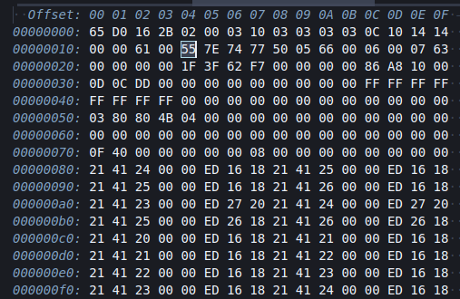
-
A7N8X-E Deluxe as an alternative for socket 462
I.nfraR.ed replied to TerraRaptor's topic in Mainboards
Attached is my custom bios for Abit NF7/NF7-S v2.0. I think it should work on v1.x as well, since I've had reports that my older mod bioses work. I will continue with testing ROMSIPs. Changelog, ROMSIP and ISA OROM source code also included in the zip. NF7D_X1-1T.zip -
A7N8X-E Deluxe as an alternative for socket 462
I.nfraR.ed replied to TerraRaptor's topic in Mainboards
Yes, it seems NVMM from AMI bios is incompatible with Award, since all 3 (4.08, 4.62 and 4.85) didn't POST on NF7 and for you. But I have the same problem with the rest which are working with failsafe and perhaps something like 166MHz FSB, but not with 200+. Will have to try with another bios or exchange the ROMSIP and see if there's a difference. While it works 260+ with NVDAMC 3.19, I could not POST at 200+ with NVMM - everything else equal. NF7 is an older board though. Maybe boot and decompression blocks matter too. Or it is just a compatibility issue with my RAM, although I have tried other modules, not just BH-5. Edit: BTW, changing BPL modules, I've noticed that the next block contains a bunch of DRAM IC part numbers, e.g. NT5DS16M8AT-6, NT256D64S8HA0G-6, M2G9JAJATT9F081AAD, MPMA82D-68KX3-MAA, MPMA82D-68KX3-MBA, HYS64D32300GU-6, DDR32Mx8AT-5, 68L3223DTM-CC4, TS64MLD64V3F5, NT256D64S88ABG-6, 64D16301GU5B, HYMD264 646B8J-D43f, MPXA82D-68KX3-MBA, MPXB62D-68KX3-MBA Maybe worth checking this module. I tried to change the whole block from another motherboard, but it didn't work. Comparing the different "tables" for a given IC between NF7 and AN7 there are some differences. Most of the bytes are the same and the length is the same. Gigabyte 7N400 has CMX256A-3200C2, CMX512-3200LL -
ROG Maximus XI
I.nfraR.ed replied to Alex@ro's topic in Skylake/Kaby Lake/Coffee Lake (-X) (Z170/Z270/Z370/X299) OC
Back when I tested XP with ACPI on Ryzen, I've made an autohotkey script (simple loop) to auto-press Enter for me, since Crosshair VI Hero doesn't have a PS/2 port. What I did is install AutoHotkey, then place the script in the startup folder, which would make it execute after booting into Windows. Then made the acronis image. All this on a board with PS/2. Now, when I restore it on the Crosshair, the script runs upon first boot and sends Enter key every 10 seconds, which activates the default "New Hardware Detected" dialogs button and hopefully it is "Next", which will install the drivers. At least it worked for me. Once you have a working usb mouse, you can stop the script and remove it from the Startup folder. I believe AHK can read window titles and button labels, then select action based on that, but I haven't spent too much time to learn it. Might help someone. enter.ahk -
A7N8X-E Deluxe as an alternative for socket 462
I.nfraR.ed replied to TerraRaptor's topic in Mainboards
Ok, just remember to rewrite the extra block with 00 on the 4.08. Edit: 4.08 doesn't work on NF7, 4.31 works with failsafe defaults only. So far all of the NVMM from AMI-based bioses don't even POST on my board. -
A7N8X-E Deluxe as an alternative for socket 462
I.nfraR.ed replied to TerraRaptor's topic in Mainboards
3 more versions. Will add if I find others. NVDAMC 3.03 05/19/2003 NVDAMC 3.16 08/18/2003 NVMM 4.31 02/24/2004 NVMM 4.08 09/29/2003 Edit: Added NVMM 4.08, but I haven't removed the block after FF AA AA BA 00 FF FF FF FF, just to try both variants, because I don't know what is it. I've removed another AMI-specific block though and padded with 00 until the end. Its release date is the same month as NVDAMC 3.19. Since the 4.35 from MSI board with NF2 bios ends with the above sequence, I guess the extra block is not needed and might even break something, but I will try it nevertheless and report back. This is the oldest NVMM I've found and there might be a chance it works fine on older boards. nvdamc-316.bpl nvmm-431.bpl nvdamc-303.bpl nvmm-408.bpl -
A7N8X-E Deluxe as an alternative for socket 462
I.nfraR.ed replied to TerraRaptor's topic in Mainboards
Yes, probably needs the newer Southbridge, or there's some other code in the bios that is required in order to make it work. 4.40 from the Abit board at least boots on NF7 with failsafe defaults, while 4.62 and 4.85 didn't even POST. I've found other 3.xx versions in some bioses and will extract them, but don't expect to be any different than what we have so far with 3.19. Haven't found a newer NVDAMC though, last one seems to be 3.19. -
A7N8X-E Deluxe as an alternative for socket 462
I.nfraR.ed replied to TerraRaptor's topic in Mainboards
NVMM 4.85 extracted from Asrock K7NF2-RAID (nForce2) AMI bios. But it didn't boot on NF7. I have copied everything between EA (this is a jmp instruction, I think) and FF AA AA BA 00 00 FF FF FF FF where it seems to end. Then padded everything with zeros until the end for the total of 19KB. nvmm-4.85.bpl -
A7N8X-E Deluxe as an alternative for socket 462
I.nfraR.ed replied to TerraRaptor's topic in Mainboards
That 4.62 didn't boot. It's 16KB vs 19KB for the rest. I also had to fill the non-overriden part with zeros. 4.40 worked, but can't POST even at manual 166MHz FSB, it only works at failsafe default for me. -
A7N8X-E Deluxe as an alternative for socket 462
I.nfraR.ed replied to TerraRaptor's topic in Mainboards
I wonder if there's some interconnection with other modules/code in the bios. And by replacing it we get the 100% out of it. -
A7N8X-E Deluxe as an alternative for socket 462
I.nfraR.ed replied to TerraRaptor's topic in Mainboards
Hmm, never thought to check that board! I can probably borrow more things from it for the NF7-S v2. Some of the Shuttle boards also use the NVMM 4.40.