-
Posts
2473 -
Joined
-
Last visited
-
Days Won
36
Content Type
Profiles
Forums
Events
Blogs
Everything posted by I.nfraR.ed
-

A7N8X-E Deluxe as an alternative for socket 462
I.nfraR.ed replied to TerraRaptor's topic in Mainboards
I've implemented a temp function which sets all these based on the selected CAS dropdown value and made some tests: Maybe we need a different sequence or set even more registers in order to make it work for all cases. Or it's just not possible. PS: 9Ah and F9h depend on the FSB as well. -

A7N8X-E Deluxe as an alternative for socket 462
I.nfraR.ed replied to TerraRaptor's topic in Mainboards
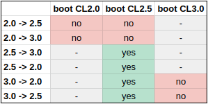
Yes, I have the same values as you. Only 2.5 -> 2.0 worked. Offset 70 and 74 (dword) bit 13 in each is Half Latency toggle. A0, A8, B0 and B8 bits 6, 5 and 4 are CAS - nforce2 supports 4 DIMMs, but B8 gets ignored in most of the boards since it's not connected. There's at least one Gigabyte board with 4 memory slots, though. -

A7N8X-E Deluxe as an alternative for socket 462
I.nfraR.ed replied to TerraRaptor's topic in Mainboards
CH sticks work with CAS3, BH are the ones that don't. I've tried to set 3.0 with a BH-5 stick and it didn't freeze. There's no difference in Pi, so I can probably only use it to detect current CAS. Changing CAS requires setting 3-4 other registers as well, I think. Will keep digging. -

A7N8X-E Deluxe as an alternative for socket 462
I.nfraR.ed replied to TerraRaptor's topic in Mainboards
You can try if it reads correct timings. Currently I've only implemented read and refresh which re-reads the timings again. I'm mostly getting these by changing a value on a running system and detecting changes in rweverything. As for Command Rate I'm not 100% sure it is correct, have to check it on a DFI board. It's read-only anyway. Yes, 90-9F is some sort of a "sensor" - values go up and down. Perhaps some voltages readings. You can actually set vdd, vdimm and FID with 8rdacore app on the fly, since it has ATXP1 control implemented. PS: Btw, I'm able to change CAS on the fly! Not sure how effective it is, but at least cpuz detects the change. Debug.zip -

A7N8X-E Deluxe as an alternative for socket 462
I.nfraR.ed replied to TerraRaptor's topic in Mainboards
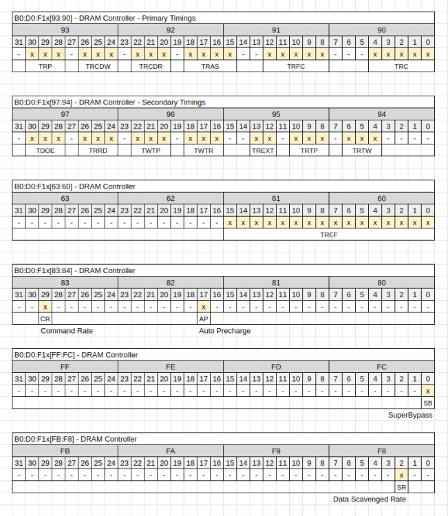
Yes, I follow that thread on your forums We (me and @TerraRaptor) were commenting your progress behind the scenes . I've even tried your modded NF7 bios and it works, but didn't see a difference in maximum stable clocks with my setup. Currently working on "documenting" all known registers. Take a look if you want and report back if you see some errors. https://docs.google.com/spreadsheets/d/1ZDST3XGq0oE7YtQxAME29RtopA8QcePCaHa2NBRHaB8/edit?usp=sharing PS: Second table, reg 94, bits [2:0] could possibly be another timing, however it might be a reserved value. AFAIK I've tried it before and it didn't accept the changed value. Also uploaded the nf7 files to my github: https://github.com/irusanov/nForce2-bios-mod -

A7N8X-E Deluxe as an alternative for socket 462
I.nfraR.ed replied to TerraRaptor's topic in Mainboards
A new tweaker coming into town ? Primary and secondary (alpha) timings read done. Will implement apply action soon. Every control reports if the value has changed and the Apply button would only set changed values.Those values are marked with yellow background. If the app reads a value (still in the defined range) that doesn't match any value in the dropdown, it will be automatically inserted in the list as a new option. For example - the default TREF on my board at 200MHz FSB seems to be 1562, while I only have a predefined 1560 in the dropdown list. Here's what I've planned DRAM primary and secondary timings drive strengths and slew rate per DIMM data scavenged rate, autoprecharge, superbypass, sync mode memory bypass Chipset AGP and PCI latencies, Side Band Addressing, CPU Disconnect, AGP Fastwrite Tweakable ROMSIP registers Profiles Predefined chipset profiles for different RAM ICs (same as @digitalbath's approach) Maybe some predefined profiles for DRAM timings as well Save/Load custom profiles Good to have SMBus control of the integrated nForce2 PLL - don't have experience there The Bad It will need .NET 2.0 framework and would have a little higher memory footprint than e.g. NF2Tweaker. Hit me with other ideas. -

scores fallen off
I.nfraR.ed replied to Matsglobetrotter's topic in HWBOT Development: bugs, features and suggestions
There's a syntax error thrown in console. You guys are using very outdated jQuery version (1.7 from 2011) when the current one is 3.4.1? I know there's no dev resource and this is a tedious task, because they are incompatible and many deprecated jQuery events need to be replaced. But all old versions have many known vulnerabilities and as you can see they stop working on modern browsers. -
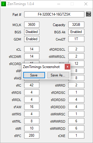
Blind testing is not recommended, since it can kill the chip. You can run the SMU scanner from SMUDebug Tool though and save the report. Sorry for the late answer. Added a screenshot button to the ZenTimings app, per popular request. Download: ZenTimings v1.0.4 (Google Drive)
-

Windows 7 x64 SP1 with integrated drivers for Zen
I.nfraR.ed replied to I.nfraR.ed's topic in Ryzen | Bristol Ridge AM4
You can try one of my tools. ZenStates: https://zenstates.protonrom.com/ SMUDebugTool: https://github.com/irusanov/SMUDebugTool/releases Due to the changes in firmware, you need to always set some values for the PBO limits. 0 was used as "auto" before, but it's now possible to set 0 as well. I'm not ready with the new version yet. You can also use SMUDebugTool if you only need to change the multiplier in OS. You can do almost everything with it, but it's all manual. First tab allows to set the multiplier easily though. It had been tested by the top US guys and it works. -

A7N8X-E Deluxe as an alternative for socket 462
I.nfraR.ed replied to TerraRaptor's topic in Mainboards
Yes, I've tested half of these, but can't confirm them all, since I stopped testing. 14h, 23h and 27h seem in line with what I've found (just from memory, I might be wrong). I have changed most of them in wpcredit and the one with most impact was the 14h, but others need thorough testing as well. -
Glad to see it is working! I'm going to update the main app, but no ETA.
-

A7N8X-E Deluxe as an alternative for socket 462
I.nfraR.ed replied to TerraRaptor's topic in Mainboards
I've tried the patcher before and have it in my archive, but I don't think it does anything interesting for our modded and newer bioses. -

A7N8X-E Deluxe as an alternative for socket 462
I.nfraR.ed replied to TerraRaptor's topic in Mainboards
Judging from the discussion in the rom.by forum, he tweaked the alpha-timings for specific Hynix chips. https://www.rom.by/forum/Moddenye_biosy_dlja_nForce_2?page=3 perhaps something to do with the module next to the BPL, like I reported here: or the BPL itself. You might find something useful by comparing the bioses. I don't have time for this now, but will get back to it some time in the future. There are many parts of the bios that are still unclear to me. I can read and understand Russian most of the time, so if you need something translated (which google translate messed up), I could probably help. Overall they don't seem to have a positive feedback on this Forsage bios. PS: He says that he fixed the timings for the specific RAM IC by reading its datasheet and changing them in the bios (probably in the block I've talked about). PS2: He also talks about a program he wrote BIOS Explorer for nForce2-bioses (BEXplo.7z) which can mod ROMSIP and CPC, but it's for 2Mbit bioses only and can't find a working link. -
ZenStates for Linux, now with a GUI. I've forked an old repo, updated it and added a GUI. Python-based. https://github.com/irusanov/ZenStates-Linux There's also a new version of the SMUDebugTool, which adds OC frequency (all cores or a chosen single core) controls and MSR read/write/scan. https://github.com/irusanov/SMUDebugTool/releases
-

A7N8X-E Deluxe as an alternative for socket 462
I.nfraR.ed replied to TerraRaptor's topic in Mainboards
Yes, I thought there's no point in changing the failsafe tables, so I left them untouched. Also tried to leave these values in the other tables, but in fact it didn't matter if I put them all the same or keep the stock values, when using the same table for all straps. What bugged me when I was trying is that some stock bioses have them mixed on some tables, like 0C10 1414. It was DFI, IIRC. Good work decoding that, though! -
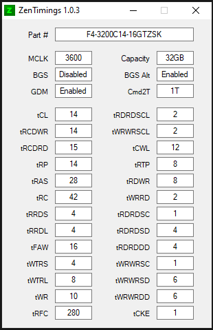
Latest version of the little ZenTimings. No plans for more updates for now, unless I find how to read FCLK, Rtt and ODT values. Should work on all Zen-based SKUs from any generations so far, including server variants. v1.0.3 adds configured DRAM frequency, total capacity and part number (read from first installed DIMM only). Download from my Google Drive -> ZenTimings
-

cnzdrn - Sempron 150 @ 6380MHz - 3443 points Geekbench3 - Multi Core
I.nfraR.ed replied to Alpi's topic in Result Discussions
Very nice. You beat me on almost everything (Pi on DDR2 is so slow compared to DDR3). The Xeon seems to be out of reach on this one though. -
Second one - yes. First one - probably not, if you've set the maximum offset in bios. There are 3 modes the CPU can operate in: Auto The CPU requests VID according to load, frequency, temperature, programmed VID, programmed (fused) power limits Offset The same as #1, but with a manual offset (either positive or negative), which doesn't mean the CPU always conforms to that - still depends on various conditions Full manual The requested VID is ignored by the motherboard and the VRM is constantly supplying the desired voltage. Changing VID in this case has no effect. I believe you're using the second case and have put the maximum positive offset. The detected VID is probably 1.100V, so the margin you have is: VIDmax - VIDdetected + VIDoffset Maximum VID for AMD is 1.55V (VID = 0). I've checked on my motherboard and maximum positive offset is +450mV. 1.550 - 1.100 + 0.450 = 0.9. So maximum possible voltage should be ~2V (not counting vdroop and LLC). If you set maximum offset from bios, then your starting point should be 1.55V, which will be mapped to the 1.100 VID in ZenStates. Assuming your max is +0.45 though. Maybe this maximum offset is calculated on the base of VIDmax - VIDdetected or it can also depend on motherboard vendor/bios. Don't have that information. One way to override the VID from ZenStates is using manual voltage from bios, but then you need to have a software designed for your motherboard, which can control its VRM IC. Perhaps I didn't fully understand the issue, so correct me if I'm wrong. As for the second thing you asked - yes, I can add a checkbox so it gets ignored when not checked. The idea is to completely rewrite the app, remove the service, remove things that don't work (e.g. Pstates, Enable/Disable SMU features), fix the power limits and add one more option (Disable PROCHOT), which should be useful on cold. Hopefully will be ready with the first version until the end of the month. PS: Btw, if you need to only set multiplier within windows, then I can give you instructions how to use the debug app for this or even strip it and expose just the multiplier thing, shouldn't take too much time. Edit: Maybe it is a good idea to replace the VID values with offsets. A little more calculations would be needed, but it's not a problem.
-
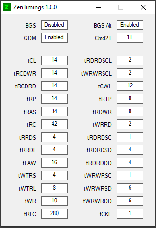
New app, ZenTimings. Verified to work on Zen, Zen+ and Zen2. Was reading wrong values on TRX40 SKUs, hopefully fixed with the 1.0.1 version. It's similar to the old Ryzen Timings Checker by @The Stilt but only includes timings I know how to read. Version 1.0.1 adds elevated privileges prompt (when needed) and a fix for reading timings on Castle Peak. Download: ZenTimings [GoogleDrive]
-

HD4870 | Oldschool boys | OVP | VT1165MF
I.nfraR.ed replied to GKirev's topic in AMD GPU Overclocking
That Volterra controller is fully programmable. What do you set voltage with? I've used the VT1165 plugin for RivaTuner in the past. There was a similar thread recently and they suggested VoltageFactory tool: https://community.hwbot.org/topic/193668-gtx-260-ocp-ovp-need/ According to the documentation, when in SVID mode, you should be able to set voltage even above 2V. As for OVP in general, the OVP trip point is usually set as an offset value (in mV) relative to the programmed VID or the nominal voltage. To lift that limit you have to re-programm the VID. On the NCP controllers, usually that's the only way. VID is set with bunch of resistors (or empty pads) each representing a single bit (0 or 1). You can configure them according to the VID table in the documentation of the controller you're working with. Normally, you don't need to touch all of the resistors. Programming a higher VID (nominal/starting voltage) lifts the trip point, although the tolerance you have is still the same if you don't have a way to increase it or disable it completely. After changing VID, you can still use that FB/Sense pin mod to increase output voltage. For example, a common NCP3588 on older cards has a non-adjustable OVP threshold. Edit: I remembered that TechPowerUp's GPU Tool also works with HD4890: https://www.techpowerup.com/download/gputool-community-technology-preview/- 1 reply
-
- 3
-

-

-
Thanks, Allen! They are designed to work on XP as well, but you'd need to update .NET Framework to 4.0 there. Can't use a lower version though, due to some features only available in .NET 4.0+. Perhaps I could try with statically linked libraries, so you don't need to install anything, but it's a bit new to me... At least with Mattise, mb vendor and model doesn't seem to matter. Perhaps a board with older SMU version might give a different result. New version of the debug tool with important bugfixes is up: https://github.com/irusanov/SMUDebugTool/releases/tag/v1.2.1 Anyone willing to test, please use this version to avoid potential problems, or at least minimize the chances. It might give some false positives for the addresses, but that's much better than BSOD or SMU lock. SMU lock can only be fixed with full power off/on cycle, even reboot from OS did not work for me. When that happens the CPU is stuck at random FID/VID state, but it probably only happens if the CPU is not in OC Mode. I've also found how to detect OC mode reliably. The old method doesn't work with the new SMU versions, thus ZenStates always thinks it is in OC mode. Next ZenStates release will be a big one, but there's a lot of work left. Those reports are definitely helping though. Most of the collected reports so far: https://github.com/irusanov/SMUDebugTool/wiki/SMU-Debug-Reports Pretty much confirming my default sets.

