I.nfraR.ed
-
Posts
2473 -
Joined
-
Last visited
-
Days Won
36
Content Type
Profiles
Forums
Events
Blogs
Everything posted by I.nfraR.ed
-
Testers are always welcome. Maybe I should create a Discord channel or something like that.
-
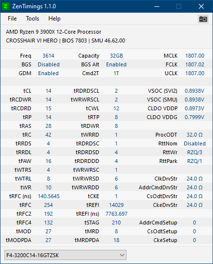
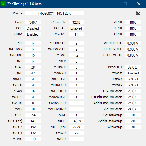
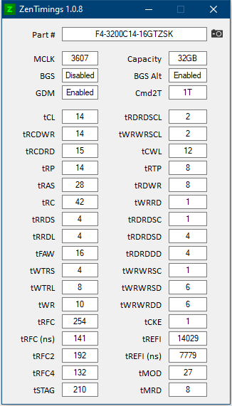
ZenTimings v1.1.0 is "officially" released. Probably ton of bugs, but will try to address them in the next versions, especially when more debug reports are available. The simple site (a copy of ZenStates with changed main color :D) is also live: https://zentimings.protonrom.com/ For debug reports, please use the tool in Tools -> Debug and attach the generated text file or copy the text directly.
-
Yes, that's possible and would like to add CLI. The linux have CLI and GUI. Currently very busy with ZenTimings, but after that I will get back to ZenStates with the new thing I've discovered recently.
-
Beta version of ZenStates with advanced Memory Controller config included. Should work on all Zen2-based CPUs and Renoir (Desktop АМ4). Readings are not realtime, but just a snapshot on app open. Don't have plans to add realtime reading, maybe a simple separate monitor app with just voltages, clocks and power. Still haven't found how to read BCLK, ACPI always reports 100. Download from GoogleDrive: https://drive.google.com/file/d/1YfHep9mX2POJhRrdEM_0WQklMDd0amZb/view?usp=sharing. 10/08/2020: Re-uploaded with a fix for first read after reboot.
-
New version of ZenTimings, with more items, Renoir and future CPUs support. https://github.com/irusanov/ZenTimings/releases Still working on the new ZenStates version. A new Linux version based on GTK3 coming too.
-
 According to my spreadsheet, it should be Athlon XP 2000+ AXDC2000DUT3C AQZFA 0343UPMW Thorton
 -
Not bad, although not sure how this translates to a DDR3 board.
-
I.nfraR.ed - FX-8350 @ 8040MHz - 9sec 437ms SuperPi - 1M
I.nfraR.ed replied to flanker's topic in Result Discussions
None of them is really a pot :D. The one over the memory is just the coldplate of Dominator water block with a styrofoam container attached with putty. The block on top is a solid glass souvenir to add some weight, because there's no mounting. -
A7N8X-E Deluxe as an alternative for socket 462
I.nfraR.ed replied to TerraRaptor's topic in Mainboards
Yes, it does. A guy from the discord channel tested it some time ago. There seems to be a difference in the chipset registers and values that work on the award boards don't work on the AMI. -
A7N8X-E Deluxe as an alternative for socket 462
I.nfraR.ed replied to TerraRaptor's topic in Mainboards
I have gained maybe 1MHz if anything at all going from air to chiller on the NB. For validation only, might help with stability when running 32M, but I haven't tried that. In my experience it doesn't scale well with cold. As for the other question - no, never had such a bad board. All my nforce2 400 ultra boards did at least 250MHz with mods. Maybe some bad capacitors? -
A7N8X-E Deluxe as an alternative for socket 462
I.nfraR.ed replied to TerraRaptor's topic in Mainboards
Keep in mind that Asus have the polarity markings for capacitors the reverse of e.g. Abit and DFI. So in fact you need to rotate the capacitor. You might know it, but just in case you've overlooked. The filled half of the circle is the positive side. Doh, is it DHL? I've had similar, when all of my contact info is replaced with something like "GDPR!!!!", so the local office can't even call me, because my mobile number is missing. Luckily I had a tracking and called the office for assistance, otherwise it would be returned back to the sender. Yeah, I've tried that long time ago and apart from being slower it did not gave me a higher FSB. I've always wanted to try 1618 or 1510 for all multipliers and see what will happen. -
A7N8X-E Deluxe as an alternative for socket 462
I.nfraR.ed replied to TerraRaptor's topic in Mainboards
I'm not sure it does anything after the DRAM is initialized. 790FX boards have it as a setting i the bios. In K8 bioses it's called "DRAM Drivers Weak Mode". Normal is the recommended setting. Some quotes from documents: -
A7N8X-E Deluxe as an alternative for socket 462
I.nfraR.ed replied to TerraRaptor's topic in Mainboards
I've tried this and some other combinations, but it always leads to a freeze. I don't know if there are other prerequisites. -
d0minat0r - Core i5 2500K @ 6382MHz - 6382 mhz CPU Frequency
I.nfraR.ed replied to 12's topic in Result Discussions
Massive! -
A7N8X-E Deluxe as an alternative for socket 462
I.nfraR.ed replied to TerraRaptor's topic in Mainboards
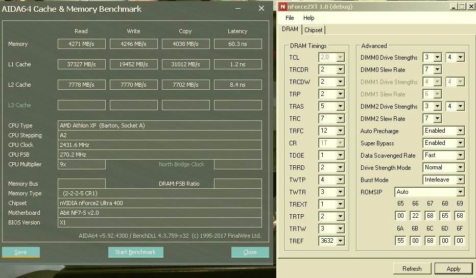
APIC off is a little more stable at high FSB and voltages for me, especially with high CPU voltage. I'm running APIC off and SSD connected to the integrated SATA on my NF7 with the images I've posted on your forum. Haven't noticed a negative effect by turning APIC off, but SATA SSD might make a difference, haven't tested. I'm currently testing the modded NF7 bios (NF7_[ED]_A6, I believe) from @digitalbath and it seems faster than mine, but it also requires a bump in VDD (chipset voltage), but I'm down to 38 27.xxx. So it seems ED is one of the fastest overall, allowing a good FSB as well. With my tweaked ROMSIP values it now runs on the lower VDD, but it would also be a little slower. These are the current ROMSIP values I'm using for 260MHz and tight BH-5 timings. It's a little bit slower, but not much, while allowing the run to complete. No 32M at 260MHz yet, though. PS: I don't see a dramatic difference in aida numbers, except Write speeds. But even with similar aida numbers one ROMSIP can be much faster that another one. We're probably hitting some nForce2 throughput, that's why aida shows similar numbers with many of the ROMSIP tables. Pi 32M tells a different story, though. -
A7N8X-E Deluxe as an alternative for socket 462
I.nfraR.ed replied to TerraRaptor's topic in Mainboards
I have experienced the crash myself and it seems to sometimes happen if you try to open the app immediately after boot. It's not related to reading timings, because I've tried without reading anything, it's related to loading and compiling the .net code to native. Maybe something is not completely ready after boot and there's some conflicting code that crashes the system. Maybe I need to have some check in place, but I don't have an idea about it. It is not that light as a native program, but can't avoid it at the moment. It only happens on first start after a fresh boot, because .net framework compiles it once. Subsequent app launches are then faster and lighter to the system. That's how .net works. There's a workaround - I can provide a mechanism to "install" that compiled native code in the cache, but this means I will have to make sure every new version of the app uninstalls it and installs the new one. If something crashes there are additional troubles. -
A7N8X-E Deluxe as an alternative for socket 462
I.nfraR.ed replied to TerraRaptor's topic in Mainboards
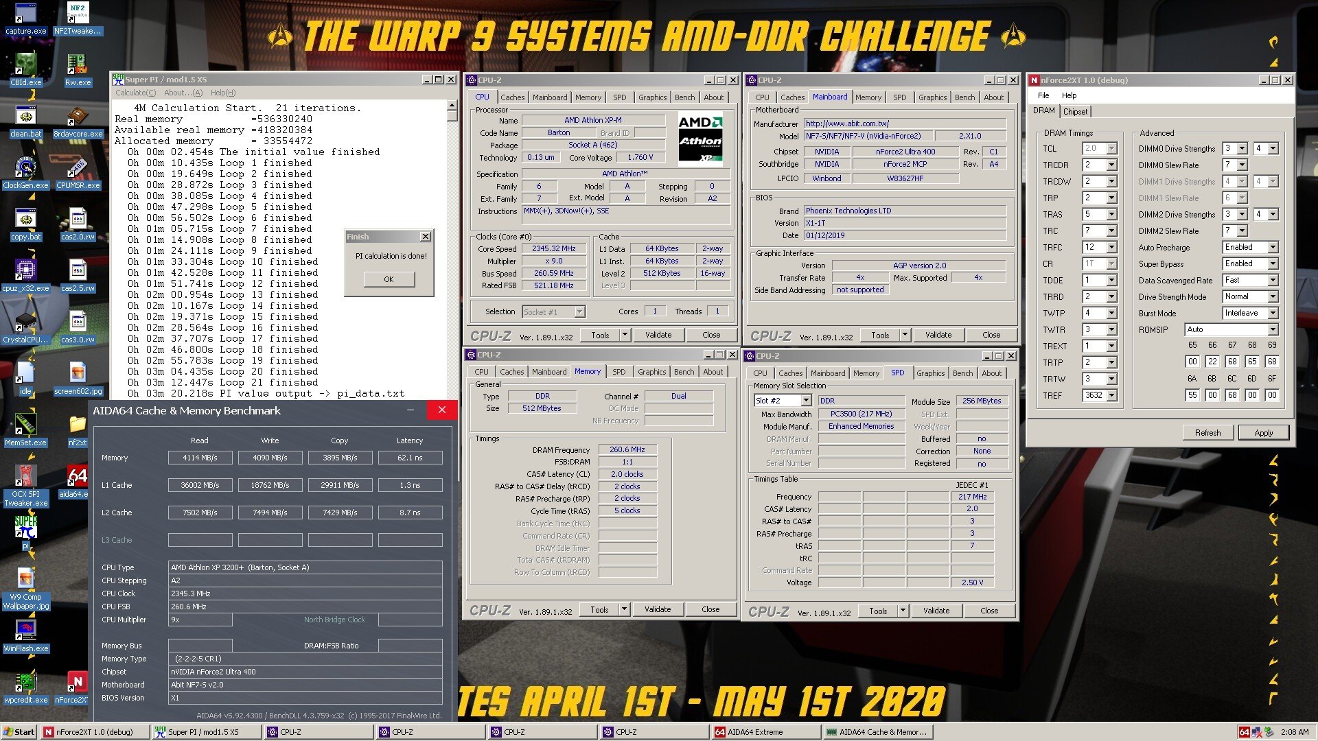
First beta is up. Everything should be functional, except profiles and items in the File menu. Latencies are now the same as in other apps, but I will have to check more boards. I'm not convinced the current mapping is right. Will work on profiles next. Had some issues with the latencies, since they are not in device #0 and write command was not working, so I had to rewrite a big part of the application and switch to other method. Don't mind the broken second image. My windows XP is really broken from some time - chkdsk is running every boot. The XP-M 2500+ I'm using is also the worst one - this is my test cpu used to check motherboards fro function and installing XP. Update: Uploaded a new version today (26 April). I've removed disabling of settings for empty slots, because it seems they get detected differently on the DFI and there's a chance you get a populated slot disabled in the app. Rendering glitch on first startup should be finally fixed. nForce2XT_1.0_beta_20200426.zip
-
A7N8X-E Deluxe as an alternative for socket 462
I.nfraR.ed replied to TerraRaptor's topic in Mainboards
It should be 0C for the AGP Controller, since I'm always reading in DWORDs (4x8 bytes, 32bits). That's how they write registers in the official documents as well. So everything in [0F:0C] range - 1st line, last column in rweverything/wpcredit in DWORD mode, is the 32bit register starting from 0xC offset. dword = double word = uint 32bit (unsigned int). 0xC, bit 0 is the least significant bit in the 32bit register. I've checked another tool - PCI Latency Tool and it lists AGP Controller Latency in the same 0xC [15:8] - 0xD portion (2nd byte) of the register, but in b2/d0/f0 - VGA Controller. So which tool/bios is right, I'm even more confused. -
A7N8X-E Deluxe as an alternative for socket 462
I.nfraR.ed replied to TerraRaptor's topic in Mainboards
I need a little help. Checking several apps and comparing with bios. According to nf2Tweaker and 8rdavcore, PCI Latency Timer is b0/d8/f0 offset 18h [31:24], although only [31:27] bits can be changed According to bios, the setting changes register b0/d1E/f0 offset 0Ch [15:8] which is AGP Controller Latency according to the other 2 apps. Could you check on Asus which register is changed? -
A7N8X-E Deluxe as an alternative for socket 462
I.nfraR.ed replied to TerraRaptor's topic in Mainboards
Two variants with tabs and everything in one page. Don't mind the reverse order of some of the timings timings on the first one, they somehow switched places. As a good news, I've solved the glitch in the rendering. It now waits until the whole layout is ready. I've also added a splash screen to show until main window pops up. I'm leaning towards the first version with tabs, although it is a little more complicated, since I'll have to check which tab is selected on Apply. Might have the rest of the controls working today.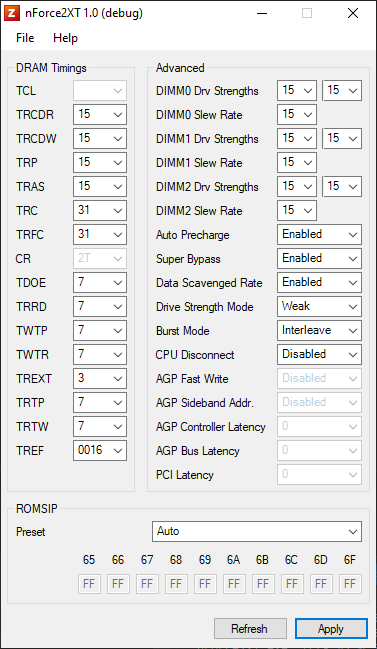
-
A7N8X-E Deluxe as an alternative for socket 462
I.nfraR.ed replied to TerraRaptor's topic in Mainboards
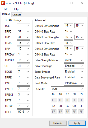
Yes, I'm thinking the original idea with 2 tabs might be a better one. Perhaps it won't hurt if the chipset settings (without ROMSIP presets) is moved to the second tab. That would save some vertical space and keep things more compact. I could probably put the romsip offset labels next to each text input, saving another line, although current one looks cleaner. Another idea I had is to change all boolean settings to on/off, instead of Enabled/Disabled, which will allow to reduce dropdown width. There are 2 exceptions though - Burst Mode and Drive Strength Mode. As you have put the columns, I can shorten the dropdowns to the default width in the second one, since they are only 2 digits. Tref is the only setting in the first one that requires 4 digits, otherwise I could shrink first column even more. I've created a discord channel to make communication easier, if anyone wants to share thoughts: https://discord.gg/hYQjbG5 -
A7N8X-E Deluxe as an alternative for socket 462
I.nfraR.ed replied to TerraRaptor's topic in Mainboards
Most of the things are already working. Disabled items are read only or not implemented yet, but getting there. DLL item seems to be unchangeable and I'm not 100% sure how it works anyway. A64 Tweaker has it, but I've never used it. Other things seem to work ok - at least they are set successfully. Adding more components made the app slower with the initial load. You might see dropdowns not fully initialized on app open, since they are all custom components. I've externalized the custom components in a separate dll and also tried to reduce memory footprint - from 14MB down to ~7MB. The plan is to also add several options to exclude things from the interface, e.g. leave just primary timings if someone doesn't want the advanced settings. If I remove DLL item, then there will be 2 empty rows in the right column, so maybe I can move something else there? It barely fits 1024x768 screen now on the vertical, but I can't really optimize the space much more than what I have currently. PS: I'm not really sure about Data Scavenged Rate, have to check on the DFI board again - might have it reversed. Not sure if Burst Mode makes sense, too. I would think you want it set to "Interleave" all the times and that seem to be the default option. nForce2XT_Debug_20200419.zip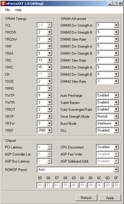
-
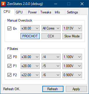
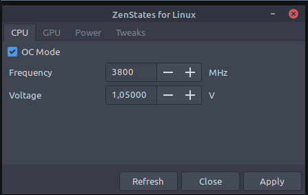
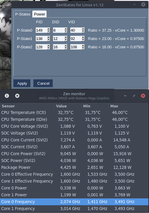
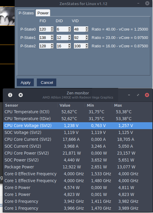
Unfortunately I haven't found any other method that works currently. I have a 240GE here, which is basically the same thing. Although you can change P0 I don't think you're using the new frequency. Have you monitored it under load? The only method I know is to reduce DID of P0 and adjust FID and VID accordingly. This allows you to go above turbo frequency, but also makes P1 and P2 useless. Example 1 - Fresh boot, stock P-States. I've adjusted P0 FID to set target frequency of 3725MHz. Although P0 changes are programmed successfully, the state is not respected. Maximum voltage is around ~1.1V and frequency doesn't go higher than stock 3500. 1.1V is the generic VID of Zen. Example 2 - P0 is changed, but this time I've dropped DID below stock, which forces some sort of a OC mode. You can now set FID and VID to desired values and overclock it as high as your CPU and cooling allows you. Once entering this state, there's no going back, you have to restart to get P1 and P2 working again. This time P0 is respected, but the CPU stays close to that P0 parameters - mine goes down to 3.6GHz when not loaded, but that's it. Screenshot is done under load. When idling the power consumption looks to be ok and unused CPU cores are probably sleeping, so that might be a good enough method, although monitoring programs still read full vCore.
-
A7N8X-E Deluxe as an alternative for socket 462
I.nfraR.ed replied to TerraRaptor's topic in Mainboards
Yes, that's what I'm thinking - placing everything on a single page. Will probably move the alpha timings beneath the main ones and use the second column for the rest of the options. The options I plan to include: Drive Strength A, Drive Strength B, Slew Rate, for each DIMM DLL [Enabled/Disabled] Burst Mode [Sequential/Interleave] Drive Strength Mode [Normal/Weak] Super Bypass Data Scavenged Rate AGP/PCI Latencies AGP Fast Write Romsip registers Not sure all of them make sense or work, but want to try anyway. Do you think 2 separate drive strengths per dimm makes sense or to include just one setting for both? -
A7N8X-E Deluxe as an alternative for socket 462
I.nfraR.ed replied to TerraRaptor's topic in Mainboards
First usable version. It's still a debug build, but you can use it for setting all the usual timings + tREF. I've disabled CAS and will remain that way, unless I found a reliable way to set it. No vendor and device check yet, so you can run even on your shiny new Ryzen under Windows 10 System requirement is .NET Framework 2.0. nForce2XT_Debug_20200416.zip