
I.nfraR.ed
-
Posts
2473 -
Joined
-
Last visited
-
Days Won
36
Content Type
Profiles
Forums
Events
Blogs
Everything posted by I.nfraR.ed
-
 You need VC++ 2005 SP1 redistributable package in order to run the patch. It didn't help with hiccups in car test when the mech is shooting. I've tested many drivers and have no solution yet.
 -
I'm lucky my HD3850 still works, although it appeared dead at first. Thanks for the patch.
-
I do. With a HD3850.
-
Windows 11 Dev vs Windows 10 Performance Test
I.nfraR.ed replied to speed.fastest's topic in Benchmark software
The popular believe is that it's basically a Win10 with a new shell and icons, so I wouldn't expect any difference in performance at this stage. -
rbuass - Phenom II X4 975 BE @ 6897MHz - 9sec 890ms SuperPi
I.nfraR.ed replied to jeremiaspc's topic in Result Discussions
It should be similar to F7e, which has some (broken) support for Vishera and I think you want older bioses for K10 anyway. -
Yes, however I have the same question about 3rd stage - are there no limits really or they were left out for some reason?
-
I know it's a language barrier, but don't know how to help you and what the problem is.
-
Good question. IMO, any customization needs to be controlled with the appropriate interface for that. I guess that feature will be back at some point, but not the free form css input. If a "theme" customization is needed, then some sort of a theme editor has to be implemented.
-
Haha, so I now know what he tried to do, either by mistake, or intentionally exploiting css injection vulnerabilities In fact I wanted to test it and report if something is wrong, but never actually got to it. Custom CSS without sanitizing it can be dangerous. PS: I think it is possible to steal someones account using that kind of XSS attack, but haven't drilled much in the topic. So..a good call, I would say.
-
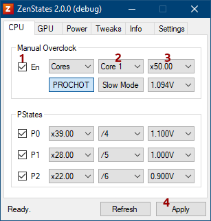
You're only interested in the "Manual OC" section at this point. Run the app, check the "En" checkbox if it is not, then select desired core index from the dropdown that currently says "All Cores", then select desired multiplier and click Apply. This should set the multiplier on selected core and you can verify it in cpuz with a right click on the frequency. It should show the desired core running at the selected multiplier. All other cores in the same CCD will drop automatically to some lower frequency. I could not make wazza work, even on XP with the classic tweaks. // Edit, I've missed the 32bit libraries in the zip, so here's a new archive with everything included. ZenStates_2.0.0_debug_20210520.zip
-
Yes, seems to be gone, but I can't really tell if something is still applied, since the site uses the custom styles from my profile Some of the styles are a little off, due to some upgrades during the years though. The logo I had is gone. PS: Actually the custom css is still applied, the background on my profile page uses black/grey shade rather than the default blue of the rest of the pages.
-
I don't really understand what you're trying to say
-
Attached is a latest build. The functionality is quite limited, but I don't have time to actually finish it. Manual OC should work though. ZenStates_2.0.0_debug_20210507.zip
-
I don't have a new Asus motherboard, but I think it can't. You can use Shamino's "OC TOOL" from the link posted in this thread, it can control cores individually: You can also use ZenStates, but I'm at work right now and have no access to my PC at home. Will attach a latest build in the evening. Keep in mind there's some relation between core frequencies and your other cores will drop to lower frequency when you set 5GHz to a single core, but that's ok for a single-threaded benchmark. As for the devices, it's always a good idea to disable everything that is not needed, such as LAN, WiFi, Audio, etc. It is not required, though.
-
I had the same error on s.775 and could not figure out why. Changed the strap and it went away. Go figure...
-
Bones - FX-8320 @ 8080MHz - 9min 50sec 391ms SuperPi - 32M
I.nfraR.ed replied to ground's topic in Result Discussions
Absolutely insane frequency. Great job! -
PBO settings don't matter when in manual overclock mode. Turn SMT off, but leave all cores enabled. Disable all unneeded devices in bios Boot and load windows at whatever all-core multiplier and voltage you can or feel comfortable with., e.g. 4.5GHz, 1.25V. For voltage, there are 2 "manual" modes, one is the full manual where the boards overrides it and you can only change from BIOS or special tools like TurboV. The other manual mode is AMD Overclocking, which can be changed from ryzen master as well. When in windows, you need to find which of your 6 cores can do 5GHz and at what voltage one by one. You may have bad sample and not all cores could do 5GHz. Increase voltage to 1.45V for example and set core #1 (second core) to 5GHz, if it doesn't crash, run superpi with affinity set to that core. If it passes, then you know core #1 is capable of 5GHz. Clock core #1 back to 4.5 and increase core #2 to 5GHz, perform the same test. Do the same for all 6 cores. If the system crashes/freezes at some point, then reboot and continue where you left. You can then test your best cores for minimum voltage as well or if none of the cores can do 5GHz at 1.45V, maybe try 1.5V. That's the general idea, to find a strong core which can do 5GHz. You don't need all the cores at that frequency, just one of them and set the superpi affinity (from Benchmate context menu) to that core, so it will only run at that thread. My CPU can run 5GHz on all cores, but cores #1 and #3 are better than the others.
-
Bones - FX-8320 @ 8304MHz - 9sec 141ms SuperPi - 1M
I.nfraR.ed replied to unityofsaints's topic in Result Discussions
Have you used the "conditioner" from Stilt? -
Haha, ok PS: Just realized all of your scores are back. Nice! I'm happy with the 2nd place for now.
-
Thanks! This CPU has potential, but either my lack of skills or the board is limiting me. Could not run any other strap and it took me a lot of time to get it 32M stable at that frequency.
-
Yes, one of Sam's binned CPUs. Didn't put much effort in this, I think ~4.5GHz 32M stable is possible on chiller. FSB-wise I'm not sure how good it is, could run around 605 with x7 multi, but I haven't really tested the board separately or played with GTLs much. Twister is on "Moderate". 1000 6-7-5 is easy with strap 200 and PL5, Twister at "Stronger" at 500 FSB, but max mem freq I could run so far is around 1030-1040, which seems to be the max of this board, at least with stock cooling and with my lack of s.775 skills. Will test it on LN2 some day, should be good for top-5 I think, maybe better.
-
POLL: CPUZ Feelz, let your opinion be known.
I.nfraR.ed replied to Splave's topic in Benchmark software
All this doesn't solve the question "But can it run Crysis at that frequency?", so why bother? I'm all for leaving it as is and don't make things more complicated. CPU-Z doesn't even show what each core is running at, it has to be modified to suit that need and I agree with others that mentioned big.LITTLE and all other complications. PS: I stand corrected, it apparently does now. It shows when I've last "benched" cpuz Technically that's not possible Rest of the cores in the same CCD will have much higher frequency. I think the maximum difference is 800MHz or something like that. Effective frequency is another thing though... but that's also applicable to all-core OC. -
Nice work! Next, try PSC/BBSE if you can do ~1100. Also, some of the Gigabyte boards are tricky with hypers and you can't POST at high mem frequency, but you can clock in windows. On my budget GB 970A-UD3 board I have to boot at 1700 and then clock up.
-
some bios and mans for old school mobos
I.nfraR.ed replied to moi_kot_lybit_moloko's topic in Old School
No need for that. Google Drive zips everything inside if you select "Download" on a specific folder. If I want to download a whole folder now it will be inflated and twice the size, because of the additional zip inside. -
The official Superpi 32M AMD Zen Low Clock Challenge thread.
I.nfraR.ed replied to d0minat0r's topic in HWBOT Competitions
To me It's just "all in", including upcoming CPUs. It's not a real competition, more like exploring the limits, thus the 1 year lifespan. It can be divided to sub-categories/stages, if there was some sort of a "official" ranking.