Crew Don_Dan Posted August 1, 2016 Crew Share Posted August 1, 2016 (edited) This thread is a copy from XS. After the hack I was afraid that this thread was completely lost, but @FUGGER was kind enough to check another back-up for me and I found the first two posts of the thread in there. I decided to share this thread with all of you to save it from being lost forever. ______________ Recently I became interested in strap tweaking again. I had only used some of them on the Commando in the past, but now I want to try them on a newer chipset. Unfortunately many of the old threads are either gone or screenshots are missing. Therefore I decided to collect all available info in this thread and copy all the screenshots to my personal imgur account. The first post will be about strap tweaking on P965, the second post will be about strap tweaking on P35/P45/X38/X48 and the third and fourth post will be about my own testing. Histoire de strap Strap tweaks were first discovered by JP on the french forum Ixtremtek on the thread Histoire de strap, which is only available on the web archive nowadays. Unfortunately only the first page of the thread is available, so I'll just copy the first post. Salut! J?ai depuis un moment d?j? entendu pas mal de chose ? propos de strap, chose qui ne me semblait pas toujours coh?rente, je me suis donc mis ? chercher ou pouvait ?tre cod? le strap dans la MCHBAR. Apr?s d?sassemblage du bios 1101 pour la P5B deluxe j?ai trouv? une adresse int?ressant, j?ai par la suite fait des comparaisons de la mchbar pour finalement m?int?resser de plus pr?s ? cette adresse FED14C00? voulant en en ?tre certain j?ai MP F?lix l?auteur de memset entre autre. Le MP: Salut! Je suis en train de faire quelques recherches pour essayer de trouver ou est localis? le strap sur P965, apr?s d?sassemblage du bios j'ai rep?rer une adresse FED14C00, qui n'est pas documenter... j'ai l'impression que c'est ou est cod? le ratio m?moire? J?ai bon ? Boblemagnifique ma envoy? deux dumps de ?a P5K: ? 555 x 6 ratio 1:1 C00 24 24 00 40 03 03 05 05 80 00 00 00 00 00 00 00 ? 267 x 6 ratio 4:5 C00 20 24 00 40 1F 1F 5B 6D 80 00 00 00 00 00 00 00 bye, a+ ...tout bon: Le registre 8bit est bien en C00h Donc 20h pour toi. 20h->0.010.0.000b 0.(010).0.{000}b La valeur entre parenth?se et le ratio m?moire, La valeur entre crochet est le fsb strap. Je suis sur la bonne route j?ai donc fait beaucoup de dumps de la mchbar ? diff?rente fr?quence et c?fficient m?moire dont voila un aper?u : http://www.overclocking-jp.eu/public...aps-ratios.png Ont peu donc voir qu?il y a trois valeurs pour le strap qui doivent ?tre (je ne serais pas affirmatif n?ayant pas la documentation confidentiel du P965?) 533, 800 et 1066. Si vous vous demand? pourquoi une valeur pour le ratio m?moire peu correspondre ? un m?me ratio c?est parce qu?il y a un changement de strap qui autorise certain ratios, ce doit ?tre ? priori comme sur d?ancien chipsets intel, les I875 / I865 en autre, ces valeurs qui sont document?? http://www.overclocking-jp.eu/public...atios/P865.png Il d'ailleurs un (vieille) article mais tr?s int?ressant pour ceux que ?a int?resserais sur x86-secret en rapport avec le sujet, dommage qu'il n'y en n'ai plus... http://www.x86-secret.com/popups/printarticle.php?id=87 Vous n??tes pas sans savoir qu?il y a une diff?rence de performance m?moire quand ont boot ? 400MHz ou 401MHz, fr?quence o? il n?y a pas de changement de strap. J?ai donc cherch? ? savoir comment rattraper ces diff?rences de perf m?moire et je suis tomb? sur le jackpot LOL J?avais d?j? un peu boss? sur les diff?rences qu?il y avait en bootant ? 400 et > Voila les diff?rences, celles int?ressante que j?ai pu trouv? jusqu'? pr?sent : http://www.overclocking-jp.eu/public...hbar_part1.png Je me suis fait une petite s?ance de bench m?moire sous Everest 3.80.948 version payante : J?ai appel? les groupes R1 R2 R3 R4 et R5 changement fait en mode 32bit. La configuration : P5B deluxe C1 Bios 1101 E6600 Le syst?me de refroidissement d?origine du chipset ? ?t? retir?, pour le remplacer par celui d?une carte m?re DFI NF4, ventilateur coup?. 2x512MB de Kingston Timings 4-4-4-12-6-35-10-10-10-10-D lien vers une photo: http://www.overclocking-jp.eu/public...s/000_1488.jpg Boot ? 401 x 9 puis passage ? 400 sous windows : http://www.overclocking-jp.eu/public...4009-stock.png Avec le tweak R5 http://www.overclocking-jp.eu/public...19_4009-R5.png Avec le tweak R5 et R4 http://www.overclocking-jp.eu/public...9_4009R5R4.png Avec le tweak R5, R4 et R3 http://www.overclocking-jp.eu/public...4009R5R4R3.png Avec le tweak R5, R4, R3 et R2 http://www.overclocking-jp.eu/public...09R5R4R3R2.png Avec le tweak R5, R4, R3, R2 et R1 http://www.overclocking-jp.eu/public...R5R4R3R2R1.png Boot ? 400 x 9 : http://www.overclocking-jp.eu/public...400x9stock.png Une fois tout les tweaks appliqu? ont peu s?apercevoir que les performances sous everest sont tr?s proche du boot ? 400MHz. Apr?s un court test de monter en fsb avec boot ? 400 et boot ? 401 plus les 5 tweaks je suis arriv? ? une m?me fr?quence, avec 1.45v au MCH, 430MHz. Voila pour le moment mes recherches toutes fra?che sur le sujet, j?ai fait d?autre d?couverte pas tr?s importante ? ce jour mais je vais s?rement jeter un ?il du cot? des dumps fait sur P5K. Un grand merci ? F?lix, j?esp?re ne pas avoir fait de b?tise en postant mon MP ? Boblemagnifique bien s?r et sans oublier Franck (de cpu-z). Commentaires bienvenus [Guide] Asus P5B Deluxe / Commando P965 JP Pmem Strap Tweaks Based on the above thread eva2000 wrote a nice guide, I'll copy the most important posts. Old boot @400FSB and clockgen/setfsb: :up: On Asus P5B Deluxe/Commando when you tip over 400FSB to 401+ FSB there's a strap change causing a massive reduction in system memory bandwidth and performance/latency. In the past to keep decent performance on Asus P5B Deluxe/Commando above 401FSB, we booted into windows at 400FSB and clockgen/setfsb our way up past 400FSB. This method required alot more vMCH (northbridge) voltage. For example, for my Asus Commando to hit 400FSB setfsb/clockgen up to 470FSB I needed bios set 1.75v vMCH voltage. JP Pmem Strap Tweaks: A few hints have been thrown around on Xtremesystems.org forums about tweaking the NB Strap settings even further within windows on the fly. Most of them refer back to jp's thread over at http://www.ixtremtek.com/forums/showthread.php?t=76 where he outlines the tweaks for Asus P5B Deluxe which from my own tests are spot on for Asus Commando as well There's 2 sets of tweaks, the original tweaks (32bit) for when you tip over the 400FSB strap change line to 401+ FSB. Then jp found some other tweaks (8bit) for at high FSB i.e. 500FSB marks. Both sets of tweaks require the use of an awesome little application called PMem. :viewfull: ----------------------------------------- Original tweaks (32bit): ----------------------------------------- Consisted of tweaking 5 memory address regions at FED14030 and FED14040. R5 - 0000000B > 0B038009 R4 - 842B4407 > 23034417 R3 - 00000000 > 37000000 R2 - 36802800 > 01002810 - boost in COPY R1 - 00025A00 > 000F5A06 - boost in READ > denotes change to Using 10x400FSB vs 10x401FSB boot as an example: 10x400FSB boot 10x401FSB boot 10x401FSB boot with JP Pmem strap tweaks applied to the 5 regions (left side is 10x400FSB boot vs right side 10x401FSB boot tweaked). ----------------------------------------- High FSB tweaks (8bit): ----------------------------------------- Used at high FSB boot configurations. Much easier to implement and remember off the top of my head FED14034h => 10 FED1403Fh => 24 * FED1403Eh => 03 FED14030h => 06 FED14040h => 09 * Memory address: FED1403Fh , when set at 23 need a lot of v-mch, when high fsb, set it to 24 is better (only if 23 is impossible) I'm using 8x500FSB 1:1 boot configuration with 1.5v vMCH northbridge voltage as an example of jp Pmem strap tweaks. Memory Read jumped from 8890MB/s to 9887MB/s (11.215% faster) Memory Write stayed approximately the same Memory Copy jumped from 7671MB/s to 9093MB/s (18.537% faster) Memory Latency tightened from 71.7ns to 57.1ns (20.363% faster) Super Pi 32M time dropped from 12m 49.281s to 12m 24.844s (3.177% faster) 8x500FSB 1:1 boot default 8x500FSB 1:1 jp Pmem strap tweaked Bios settings used: [b]Extreme Tweaker:[/b] AI Tuning: Manual CPU Frequency: 500FSB DRAM Frequency: DDR2-1000MHz (1:1 Divider) PCI Express Frequency: 100 PCI Clock Synchronisation: 33.33 Spread Spectrum: Disabled CPU Vcore Voltage: 1.575 FSB Termination Voltage: 1.4 NB Vcore: 1.5 Memory Voltage: 2.2 DDRII Channel A REF Voltage: Auto DDRII Channel B REF Voltage: Auto DDRII Controller REF Voltage: Auto SB Vcore (SATA, PCIE): 1.6 SB Chipset Voltage: 1.225 Asus C.G.I.: Disabled Static Read Control: Disabled Configure DRAM Timing by SPD: Disabled - DRAM CAS# Latency: 4 - DRAM RAS# to CAS# Delay: 4 - DRAM RAS# Precharge: 4 - DRAM RAS# Activate to Precharge: 5 - DRAM Write Recovery Time: 3 - DRAM TRFC: 30 - DRAM TRRD: 3 - Rank Write to Read Delay: 10 - Read to Precharge Delay: 10 - Write to Precharge Delay: 10 Legacy USB Support: Disabled CPU Configuration Modify Ratio Support: Enabled - Ratio CMOS Setting: 8x C1E Support: Disabled Max CPUID Value Limit: Disabled Vanderpool Technology: Disabled CPU TM function: Disabled Execute Disable Bit: Disabled PECI: Disabled End result is something like this Original post http://www.ixtremtek.com/forums/showpost.php?p=1544&postcount=18 I've performed a little bit of testing yesterday. Here are the results. M/B:ASUS P5B-Deluxe 1.03G P965C1 rev., Vcore, Vdroop, Vdimm, Vmch mods CPU:Intel Core2 E6700 L633A550 CPU cooling:Watercooling Alphacool Memory:Wintec PC2-8000 C5 1024MBx1 VGA:Jaton 8600GS HDD:Western Digital 80GB Power Supply:Antec TP 550W Vcore:1.390V(Bios) Vdimm:2.62V(Actual) FSB Termination Voltage:1.45V NB Voltage:1.71V(Actual) OS:Windows Server 2003 Boot clocks: 570FSBx6 1:1 Max FSB with original 1333 strap: 589FSBx6 validated; 591FSBx6 frozen screen CAS Latency: 4 RAS to CAS Write Delay: 4 RAS to CAS Write Delay: 4 RAS Precharge: 4 Precharge Delay: 8 All Precharge to Activate: 4 Refresh Cycle Time: 30 Performance Level: 10 Write to Precharge Delayed: 11 Write to Read Delayed: 10 Activate to Act. Delayed: 10 Read to Write Delay: 8 Read to Precharge: 8 All Precharge to Refresh Delay: 4 Precharge to Precharge Delay: 2 Max FSB with modded 1333 strap: 584FSBx6 validated; 585FSBx6 frozen screen CAS Latency: 4 RAS to CAS Write Delay: 4 RAS to CAS Write Delay: 2 RAS Precharge: 4 Precharge Delay: 8 All Precharge to Activate: 4 Refresh Cycle Time: 25 Performance Level: 1 Write to Precharge Delayed: 11 Write to Read Delayed: 10 Activate to Act. Delayed: 3 Read to Write Delay: 7 Read to Precharge: 2 All Precharge to Refresh Delay: 4 Precharge to Precharge Delay: 2 [missing pic] [missing pic] http://valid.x86-secret.com/show_oc.php?id=237597 Strap modding study: These figures show the Everest benchmark results obtained after modding the mchbar addresses the one after the other. Only results with significant changes are given. [missing pic] Mean = 8698.22 SD = 95.73 VAR = 9163.59 Best = FED14040h = 08 => 8760 MB/s FED14030h and FED14040h look like to have a significant impact on memory read performance. [missing pic] Mean = 7196.94 SD = 43.89 VAR = 1926.53 Best = FED14030h = 06 => 7317 MB/s FED1403Eh and FED14030h look like to have a significant impact on memory copy performance. BTW changing other addresses cause this improvement to be moderated and stabilized within 7170 MB/s to 7200 MB/s. A bit strange IMO. [missing pic] Mean = 82.27 SD = 7.04 VAR = 49.57 Best = FED1403Bh = 37 => 76.8 ns FED14040h and FED1403Bh look like to have a significant impact on memory latency performance. [missing pic] Mean = 26790.22 SD = 45.57 VAR = 2076.30 Best = FED14040h = 09 => 26825 MB/s FED14040h looks like to have a significant impact on L2 Cache read performance. [missing pic] Mean = 21678.11 SD = 48.68 VAR = 2369.99 Best = FED14042h = 03 => 21721 MB/s FED14042h and FED14040h look like to have a significant impact on L2 Cache write performance. [missing pic] Mean = 29395.69 SD = 53.64 VAR = 2877.66 Best = FED14040h = 08 => 29444 MB/s Mostly FED14040h but also a bit lesser FED14042h look like to have a significant impact on L2 Cache copy performance. [missing pic] Mean = 4.93 SD = 0.27 VAR = 0.07 Best = FED14042h = 02 = FED1403Bh = 37 => 4.7 ns FED14040h looks like to have a significant impact on L2 Cache latency performance. We could notice the small improvement given by FED14042h and FED1403Bh. Hey before thanks for the info.. alot of work done there When i did above tests at 500-501FSB, FED1403Bh was already set to 37 on Asus Commando. Was it different by default on P5B Deluxe or just it changed at 570+ FSB (never got a cpu that far) ? That's really interesting I've got no clue; I'm gonna give it a glance. I'm about to finish a small single stage to make some tests @600FSB. It's built with a rotary cp but the cap tube is so short that I'm not aiming for very cold temps but strong hold of load. I hope to be able to use strap tweaks even with very high FSB values. E8500 6GHz Benchable Club NewBeetle found some very interesting settings he posted in this thread. Then, I tried "JP Pmem Strap Tweaks".It accelerated by 4%. Thank you so much for your advice, dinos22-san!!! :up: Cheers for wonderful "JP Pmem Strap Tweaks"! :toast: :toast: :toast: modPI 8M : 1m42.078s @5890.3MHz (FSB620.0MHz x 9.5) Setup CPU:Core2 Duo E8500#2 Q745A703 M/B:ASUS P5B Deluxe WiFi Rev.1.04#6 vmod / BIOS:1223 M/B Bed:V-TEC ARC Bed Rev.3.3 CPU cooling:MaxxNeo + LN2 / Temp:-145C NB cooling:Tara-chan 1st + LN2 / Temp:-45C SB cooling:stock Mem:Team PC2-8500 C4 1GB x2 VGA:MSI NX7900GTO 512MB PCI-EX HDD:Maxtor 6Y080P0 (IDE) PSU:Antec Quattro 1000 OS:Windows Server 2003 CPU Multiplier:x9.5 FSB:550MHz @boot CPU/Memory:1:1 PCIExpress:100MHz PCI Clock:33.33Mhz Vcore:1.912V(CPU-Z) Vdimm:2.67V(Actual) FSB Termination Voltage:AUTO NBVcore:1.65V(Actual) SBVcore:AUTO ICH Chipset Voltage:AUTO But my best DDR2 memory died in this test. I secede from the front for a while. : DEWA DEWA NewBeetle Congrats Newbeetle-san Just curious; you're running FED14034h to 12: did you try setting it to 10 (high vMCH required) you're running 03Bh to 00: did you try setting it to 37? you're running 03Eh to 04: did you try setting it to 03? you're running 03Fh to 26 (really too high IMHO; but maybe required for actual FSB): did you try setting it to 23 (needs very high vMCH) or 24? you're running 040h to 10: did you try setting it to 08 or 09? you're running 041-043h to 00 00 00: did you try setting it to 80 03 0B? If you need help or something; just frop me a pm. Thank you so much, before-san. I study "JP Pmem Strap Tweaks" just now! First, I learnt it this page. http://www.i4memory.com/showthread.php?t=4268 And setting like this. FED14034h => 10 FED1403Fh => 24 FED1403Eh => 03 FED14030h => 06 FED14040h => 09 But it did not work FSB600MHz over in my system..... And, when I change the following values, it worked by chance. : FED14034h => 12 FED1403Fh => 26 FED1403Eh => 04 FED14030h => 06 FED14040h => 10 I try and error because it seems not the best value. So I will try your setting at once! :up: Of course, I need help. I will sent PM to you. Again thank you so much for your kindness. :bows: Best Regards NewBeetle You're welcomed Newbeetle-san. It's possible that your actual values are the best for 620FSB. I personally have used tighter values up to 605FSB or so, but never had any chance to do it at 620FSB due to a combination of CPU/MOBO limitation. So; I'm gonna reply your pm ASAP. PS: If you want to ask JP directly about these offsets; you may wish to post here http://www.ixtremtek.com/forums/showthread.php?p=1567 Congrats. :up: Does anyone yet know what those registers each actually represent? What are they controlling exactly? Chipset FSB to strap related. Very important on P965; less on newer chipsets due to the nature of straps which is now memory divider dependent. Thanks Xavier. I knew that much : It has to represent some parameter the MB MFG knows or they couldn't have coded for it especially the chipset teams. Chipset is old and I was away from online involvement when it was in use and released or I'd experiment with it to find out. Thank you very much, before-san. I have just recieved your PM. I will try your setting ASAP! :up: Thank you, KTE-san. Now, I have got new DDR2 memory. And I can get another result by "JP Pmem Strap Tweaks(not best setting)". :up: By NewBeetle Setup CPU:Core2 Duo E8500#2 Q745A703 M/B:ASUS P5B Deluxe WiFi Rev.1.04 #6 vmod / BIOS:1223 M/B Bed:V-TEC ARC Bed Rev.3.3 CPU cooling:MaxxNeo + LN2 / Temp:-150C NB cooling:Tara-chan 1st + LN2 / Temp:-45C SB cooling:stock Mem:Team PC2-8500 C4 #2 1GB x2 VGA:MSI NX7900GTO 512MB PCI-EX HDD:Maxtor 6Y080P0 (IDE) PSU:Antec Quattro 1000 OS:Windows Server 2003 CPU Multiplier:x9.5 FSB:550MHz @boot CPU/Memory:1:1 PCIExpress:100MHz PCI Clock:33.33Mhz Vcore:1.944V(CPU-Z) Vdimm:2.60V(Actual) FSB Termination Voltage:AUTO NBVcore:1.70V(Actual) SBVcore:AUTO ICH Chipset Voltage:AUTO "JP Pmem Strap Tweaks (not best setting)" FED14030h => 06 FED14034h => 12 FED1403Bh => 37 FED1403Eh => 03 FED1403Fh => 26 FED14040h => 08 FED14041h => 80 FED14042h => 03 FED14043h => 0B hexus_pifast : 16.08s @5828.1MHz (FSB613.5MHz x 9.5) Thank you, Felipe-san. Finally i got it. hexus_pifast WR : 15.86s @5928.4MHz (FSB624.0MHz x 9.5) [missing pic] Setup CPU:Core2 Duo E8500#2 Q745A703 M/B:ASUS P5B Deluxe WiFi Rev.1.04 #6 vmod / BIOS:1223 M/B Bed:V-TEC ARC Bed Rev.3.3 CPU cooling:MaxxNeo + LN2 / Temp:-155C NB cooling:Tara-chan 1st + LN2 / Temp:-45C SB cooling:stock Mem:Team PC2-8500 C4 #2 1GB x2 VGA:MSI NX7900GTO 512MB PCI-EX HDD:Maxtor 6Y080P0 (IDE) PSU:SilverStone OP1200 OS:Windows Server 2003 CPU Multiplier:x9.5 FSB:550MHz @boot CPU/Memory:1:1 PCIExpress:100MHz PCI Clock:33.33Mhz Vcore:1.952V(CPU-Z) Vdimm:2.60V(Actual) FSB Termination Voltage:AUTO NBVcore:1.70V(Actual) SBVcore:AUTO ICH Chipset Voltage:AUTO "JP Pmem Strap Tweaks" / Special Thanks, before-san FED14030h => 06 FED14034h => 12 FED1403Eh => 04 FED1403Fh => 25 FED14040h => 08 DEWA DEWA NewBeetle You're very welcome NewBeetle-san :toast: Congrats for this amazing WR. :up: STRAP-мод Topmods posted an article about strap tweaking. Core2Duo Е6400 (маркировка L631B317) ПаÑта Coollaboratory Liquid Pro Asus Ð 5Ð’ Deluxe rev 1.03G bios1215 pencil Vdroop mod 2Ñ…1Гб Corsair 8500C5D rev 1.2 XFX 8800GTX 675/1620/1900 150Gb Raptor WD1500AHFD Dvd-rw Pioneer 111D Thermaltake Damier V6000A Enermax ELT500AWT Since he explaines the process very thorougly, I'll just summarize his settings. The testing was done at 400MHz and 500MHz FSB. FED14030h => 06 (was 00) FED14034h => 10 (was 00) FED1403Eh => 03 (was 2B) FED1403Fh => 24 (was 84) FED14040h => 09 (was 0B) FED14030h => 06 (was 00) FED14034h => 10 (was 00) FED1403Eh => 03 (was 2B) FED1403Fh => 23 (was 84) FED14040h => 09 (was 0B) FED14030h => 06 (was 00) FED14032h => 0F (was 02) FED14034h => 10 (was 00) FED1403Bh => 37 (was 00) FED1403Ch => 17 (was 07) FED1403Eh => 03 (was 2B) FED1403Fh => 24 (was 84) FED14040h => 09 (was 0B) FED14030h => 06 (was 00) FED14032h => 0F (was 02) FED14034h => 10 (was 00) FED1403Bh => 37 (was 00) FED1403Ch => 17 (was 07) FED1403Eh => 03 (was 2B) FED1403Fh => 23 (was 84) (needs high Vnb ~1.77V) FED14040h => 09 (was 0B) A little comparison at high FSB clock to show the difference: Stock: Edited: Miscellaneous No idea where this screenshot came from, but I found it on my HDD. Edited August 1, 2016 by Don_Dan 1 Quote Link to comment Share on other sites More sharing options...
Crew Don_Dan Posted August 1, 2016 Author Crew Share Posted August 1, 2016 (edited) [Guide] Asus P5B Deluxe / Commando P965 JP Pmem Strap Tweaks youngpro posted this in the above thread. sorry to be a thread digger but ive been doing some testing with values on the x38t-dq6 board, i get a 5% memory performance jump when tightening up FED1403Fh to 23 on this motherboard, great to finally get time to test these things! FED1403Fh => 23 Biostar Tpower P45 first look with Team.AU youngpro posted some more info in his thread about the Biostar TPower I45. mchbar edits, i based on newbeetles testing, 00 set to 06 and 08 set to 26 for fed14030 register, if i set all of the known mchbar edits to increase fsb i got lower fsb, these two gave me my max fsb achievable, this cpu maxed at 470~ on gigabyte/foxconn/asus x48t boards, 465 on p35t-dq6, so reasonable fsb gain there on the biostar board, this was a review board, i think before/newbeetle posted some good mchbar edits, also eva put up a big thread here giving information on how to do it and fsb gains/performance increases FED14030h => 06 FED14038h => 26 OPB 2008週末極é™è¬›å ‚; fsb651é”æˆ-P45çš„MCHBAR Tweak探索 OPB shared some settings for Biostar P45 in this thread. 大家好,狂少剛好利用美國國慶å‡æ—¥çš„機會來跟大家討論一下:P45 mch的變相效能調法 之å‰åœ¨å’Œè€å¤–朋å‹æåŠp45åªæ˜¯ç´™è€è™Ž(fsb高,其它無用)時 çªç„¶å›žæƒ³åˆ°p965當åˆå‰›å‡ºçš„ç‹€æ³å¾ˆåƒ 後來有些人是使用一種å«Pmem的工具去修改其MCH(北橋的記憶體控制碼) barä¸èˆ‡è¨˜æ†¶é«”相å°æŽ§ç®¡FSBçš„ä½å€,使在高fsb時還是å¯ä»¥æ“有高的讀寫效能 ç‹‚å°‘åšäº†ä¸€äº›å°æ¸¬,也希望若有p45çš„åŒå¸ä¹Ÿèƒ½é€ä¸€å°è‰ æ—¥å‰æˆ‘也有ç¨å¾®è«‹æ•™éŽOskar,已經確èªç„¡ç–‘,這方法的確是模擬p965çš„MCHbaræ ¡èª¿ 來使用在P45上,雖說效能ä»æœ‰å·®è·,但是我相信還會在改善 測試環境: CPU: Intel E8400 cooler: thermalright u120e power: PC P&C 1200w turbo cool mobo: Biostar I45 tpower bios 630 HD wd velociRaptor 300g VGA HD480 å–®å¡ RAM: Team Group pc 6400 來,在圖ä¸å¤§å®¶å¯ä»¥çœ‹åˆ°ç‹‚少使用Pmemé€™å·¥å…·ä¾†æ ¡è¨‚8bit hex code 在讀寫增進方é¢, 我們需è¦æ‰¾åˆ°"FED14030-0f這ä½å€" 他的原始è¨å®šåœ¨æ¯ä¸€å®¶moboå» éƒ½æ˜¯ä¸ä¸€æ¨£, biostar是這樣: default :84 æˆ‘å€‘é †ä¾¿ä¾†çœ‹å®ƒçš„everesté »å¯¬: [missing pic] å†ä¾†æˆ‘們拿Intel p965çš„FED140300fçš„24來比å°, [missing pic] 如果我們å†æŠŠä»–é™åˆ°22.. 如何..å…‰æ˜¯é »å¯¬å°±å¤šå¤šå°‘? 那記憶體讀寫改善,spi會ä¸æœƒæ€Ž? ä¸æœƒ,é‚£ä¸è¦çŽ©é›»è…¦äº†... 先看default: [missing pic] å†çœ‹22... [missing pic] FED1403Fh => 22 Some QX9650 results with MSI P35D3 Platinum, STT DDR3 1600 and 2-Stage Cascade before shared some info in his thread about the MSI P35D3. I've got tons of things to do; so I didn't had the time to bench more on this board. BTW; I've added a second solid aluminium capacitor to the vFSB area; and made some investigations on MCHBAR coding. So; the memory bandwidth/latency is definitely better while booting at 399FSB with FSBSEL jumpers set to 333 strap. Of course, this setting also adds more stress on the MCH, and obviously varies with CPU multipliers. That's odd indeed. In fact, stability is quite good with 10x multiplier, but becomes bad with 13x multiplier using the exact same bios settings... Why? I've made registers dumps to perform comparisons. Here are the differences (quite a lot for only a multiplier difference ) 399FSB MCH x13 x10 140 FB FD 141 20 60 142 1F 1E 148 61 E1 149 59 38 184 01 61 185 9D 15 188 F4 E6 189 D1 11 198 00 12 1A8 01 02 24A C6 C7 36E 4C C9 36F C6 C4 52C 12 00 52D 33 21 530 65 43 531 88 66 A0C 76 77 A14 07 08 BC1 49 47 BC3 49 47 BD8 17 1B BDA 17 1B I'll not come to details, but the first one which shines on my eyes is offset MCH+24A (FED1424Ah). Just check line starting with 24A. In fact, as you can see offset 24A = C6 with CPU multiplier 13x, and = C7 with CPU multiplier 10x. What does that mean? So, let me tell you. AFAIK this particular offset is where the CAS Latency (tCL) timing is hard-codded for memory Channel #0. It's a Read/Only 8bits value which requires electrical reboot to be changed. Basically, C0 = tCL1, C1 = tCL2, C2 = tCL3, etc. to C6 = tCL7 and C7 = tCL8. So, as can be seen tCL for channel #0 is 8 while booting at 399FSBx10 but 7 while booting at 399FSBx13. That's odd; knowing that I set tCL to 7 in the bios... : Then, I've tried to boot at 399FSBx13 with tCL set to 8 in the bios; and the system became stable :yepp: 24A offset was correctly set to C7, just like while booting at 399FSBx10 with tCL set to 7 in the bios. Guess there's a matter of bios coding here. BTW dunno why, but LargeSystemCache (LSC) = 1 causes unstability again. :ROTF: The memory controller might be out of breath. What's interesting to note is that Spi32M can pass successfully with multiplier 13x and LSC=1 if I don't boot at 399FSB. It looks like something related to MCH data transfer limitation. I'll try with more Vmch; but I don't really like it. Actual tests were performed with 1.75Vmch (DMM). Click the thumbnail to view full-size image [missing pics] M/B:MSI P35D3 PlatinumCPU:Intel Core Extreme QX9650ES C738A551CPU cooling:2 Stage Cascade "Petite Bertha"Memory:G.Skill 2x12800CL7-1GBHZVGA:Asus HD3870HDD:Western Digital 80GBPower Supply:Antec TP 550WVcore:1.69v(Actual), 1.85v(BIOS)Vdimm: 2.10v(Actual), 2.25v(BIOS)Vmch: 1.57v(Actual), 1.65v(BIOS)OS:Windows 2003 Server (maxmem=600)Misc.: MCHBAR mods (030-043h, C50-C57h, 23Eh/63Eh, 258-258h/658-659h) Thx to both JP and Roger for their help. Now... I can increase the bandwidth in a very significant way. Any ideas about these X38 MCHBAR registers? before, FELIX and The_Stilt shared lots of info on different registers in this thread. I'd like to know the purpose of these two registers: For Channel 0: MCH + 540h to 5CFh For Channel 1: MCH + 940h to 9CFh Can't figure out what both registers stand for... They look to play a big role in memory bandwidth and latency; and obviously in system stability as well. BTW, Intel X38 datasheet doesn't mention them. when do they change? Dunno if it's revealant or not, but here's what I've checked recently. [missing pic] Points to note: BIOS 0124 is a pre-45nm version for the P5E3 WS Pro BIOS 0306 is a post-45nm version for the P5E3 WS Pro Changes between both BIOS take place into columns 00, 04 and 0C. Column 04 for BIOS 0124 isn't coded? or coded to 00 which results in crappy bandwidth and latency. Applying column 04 offset values of BIOS 0306 to BIOS 0124 MCHBAR allows to increase bandwidth and latency in a very significant way. For instance at 399FSBx13(QX9650) 1:2 7-6-5-15, setting 05 to 564h into BIOS 0124 MCHBAR gives the following results: 10874MB/s vs 10504MB/s (memory read), 9905MB/s vs 9866MB/s (memory copy), 48.8ns vs 51.3ns (memory latency), 2m00.966s vs 2m02.640s (Super PI 8M) interesting... could it be the registers for the trd phases maybe? Yeah maybe. Not sure how column 04 coding works... Tried Spi 32M with 544h, 564h, 944h and 964h all set to 05, and computation was faster (by about 2s) than with all these set to 03. The higher the better? Or each one must be individually considered? in everest bandwidth trd+1 = +150mb/s iircthis sounds like a very nice tweak then did you check if those register change if you set a different pl? or maybe if you switch from cmd 1t to 2t? Not tried yet. Another register which could be of interest is C50h to C57h. Credits for this discovery belongs to my friend JP (aka Learn). Basically it changes accordingly to DRAM dividers; BTW you can improve it manually. According to JP's first thoughts, 1:1 related setting might be the best for all dividers in term of bandwidth size (FF FF FF FF 00 00 FF FF). BTW after playing with it a bit; it seems me something better might exist (for instance 05 03 03 FF FF FF 01 FF for 1:2). Anyway, that's another history. : very interesting xavier!thanks for sharing :toast: you should write a bandiwdth tweaking article if you have the time i can help you and run some tests as well, just tell me what to do Yeah why not BTW, for most tweaks I don't feel really confident. MCHBAR is so vast and things move from a boot to another, making some offsets important and others useless, and reversely. The matter is, the Intel datasheets (at least those I know, those available to public) are so succint and most of the interesting registers aren't mentioned. If you wanna try something, I encourage you to test C50 to C57h register. It usually gives a nice boost: a good value is FF FF FF FF 00 00 FF FF. Additionally, 03Fh is a nice offset as well. Setting it to 22 or 23 is nice (sometimes it's already coded to 13, and that's look like 23... not so much difference IMHO). TBH before PL was associated to tRD (I'm still not so sure indeed), I was thinking about 03Fh for this role :yepp: In fact, it's much more a MCH related timing as it only consists in a single offset while "Perfomance Levels" are individually coded for each channel. Like any other DRAM timing, PL offsets are among the DRAM registers (highlighted in yellow here; just prior to 86 which is offset 24Ah, the one to control CH0 tCL -here, 86 = tCL7-) [missing pic] It's a matter of balance, there are offsets which stress more the MCH, and others which stress more the DRAM. For instance, on a P5B P965, if you want to run 23 setting for 03Fh at lets say 550FSB, you need a significantly higher vMCH than with 24... But if you want to decrease the PL, you need to increase vDDR... I've already sent him a pm about something else, but unfortunately he never answered. I guess that he doesn't come here too much. Anyway, concerning the purpose of this thread, I'm guessing those registers are for the Advance Skew. I'm not sure how to use it properly BTW. clock skew aka read/write levelling? ...if it can help you: -PL/tRD is at Offset 248[12-8] for channel A and 648[12-8] for channel B -tCL is at Offset 264[21-16] for channel A and 664[21-16] for channel B and I made some search recently for tRD Phase Adjust using Everest: -tRD Phase Adjust is at Offset 23C[19-16] for channel A and 63C[19-16] for channel B; (very unstable timings) Thanks for your input. I'm a bit surprised BTW. As you can see in the previous table PL for CH0 is at offset 249h; 248h is empty actually. Same for tCL; just check these dumps. tCL changes at 24Ah / 64Ah, (tCL3 = C2; tCL4 = C3; etc.) while 264h / 664h is staying to 78 (at least until tCL6). Maybe I'm missing something. Memory Frequency 267.3 MHz (1:1) CAS# 3.0 RAS# to CAS# 4 RAS# Precharge 4 Cycle Time (tRAS) 12 Command Rate 2T 200 00 00 00 00 08 00 10 00 00 00 02 02 00 00 00 00 210 00 00 00 00 00 00 00 00 00 00 00 00 00 00 00 00 220 17 11 00 58 01 02 24 0C 00 00 00 00 00 00 00 00 230 00 00 00 00 00 00 00 00 00 00 00 00 89 7A 00 00 240 00 11 00 01 10 23 11 00 00 06 C2 0E 00 11 30 00 250 D5 02 1E 88 26 00 68 44 46 95 08 1E 08 0C A5 15 260 91 3D C7 0B 78 00 0C 13 00 28 CA CF 33 BF 02 03 270 00 1E 55 01 01 A9 08 00 81 18 14 88 41 00 00 00 280 00 00 00 00 00 00 00 00 00 02 04 08 10 20 40 FF 290 1C 09 F2 04 44 00 00 00 00 00 00 00 68 06 00 00 600 00 00 00 00 08 00 10 00 00 00 02 02 00 00 00 00 610 00 00 00 00 00 00 00 00 00 00 00 00 00 00 00 00 620 17 11 00 58 01 02 24 0C 00 00 00 00 00 00 00 00 630 00 00 00 00 00 00 00 00 00 00 00 00 89 7A 00 00 640 00 11 00 01 10 23 31 00 00 06 C2 0E 00 11 30 00 650 D5 02 1E 88 26 00 68 44 46 95 08 1E 08 0C A5 15 660 91 3D C7 0B 78 00 0C 13 00 28 CA CF 33 BF 02 03 670 00 1E 55 01 01 A9 08 00 81 18 14 88 41 00 00 00 680 00 00 00 00 00 00 00 00 00 02 04 08 10 20 40 FF 690 1C 09 F2 04 44 00 00 00 00 00 00 00 68 06 00 00 Memory Frequency 267.3 MHz (1:1) CAS# 4.0 RAS# to CAS# 4 RAS# Precharge 4 Cycle Time (tRAS) 12 Command Rate 2T 200 00 00 00 00 08 00 10 00 00 00 02 02 00 00 00 00 210 00 00 00 00 00 00 00 00 00 00 00 00 00 00 00 00 220 17 11 00 58 01 02 24 0C 00 00 00 00 00 00 00 00 230 00 00 00 00 00 00 00 00 00 00 00 00 89 7A 00 00 240 00 11 00 01 10 23 11 00 00 07 C3 0E 00 11 35 00 250 15 03 1E 88 26 00 68 44 46 A5 08 1E 08 0C A5 15 260 91 3D C7 0B 78 00 0D 13 00 28 CA CF 33 BF 02 03 270 00 1E 55 01 01 A9 08 00 81 18 14 88 41 00 00 00 280 00 00 00 00 00 00 00 00 00 02 04 08 10 20 40 FF 290 1C 09 F2 04 44 00 00 00 00 00 00 00 68 06 00 00 600 00 00 00 00 08 00 10 00 00 00 02 02 00 00 00 00 610 00 00 00 00 00 00 00 00 00 00 00 00 00 00 00 00 620 17 11 00 58 01 02 24 0C 00 00 00 00 00 00 00 00 630 00 00 00 00 00 00 00 00 00 00 00 00 89 7A 00 00 640 00 11 00 01 10 23 31 00 00 07 C3 0E 00 11 35 00 650 15 03 1E 88 26 00 68 44 46 A5 08 1E 08 0C A5 15 660 91 3D C7 0B 78 00 0D 13 00 28 CA CF 33 BF 02 03 670 00 1E 55 01 01 A9 08 00 81 18 14 88 41 00 00 00 680 00 00 00 00 00 00 00 00 00 02 04 08 10 20 40 FF 690 1C 09 F2 04 44 00 00 00 00 00 00 00 68 06 00 00 Memory Frequency 267.3 MHz (1:1) CAS# 5.0 RAS# to CAS# 4 RAS# Precharge 4 Cycle Time (tRAS) 12 Command Rate 2T 200 00 00 00 00 08 00 10 00 00 00 02 02 00 00 00 00 210 00 00 00 00 00 00 00 00 00 00 00 00 00 00 00 00 220 17 11 00 58 01 02 24 0C 00 00 00 00 00 00 00 00 230 00 00 00 00 00 00 00 00 00 00 00 00 89 7A 00 00 240 00 11 00 01 10 23 11 00 00 08 C4 0E 00 22 39 00 250 55 03 1E 88 26 00 68 44 46 B5 08 1E 08 0C A5 15 260 91 3D C7 0B 78 00 0E 13 00 28 CA CF 33 BF 02 03 270 00 1E 55 01 01 A9 08 00 81 18 14 88 41 00 00 00 280 00 00 00 00 00 00 00 00 00 02 04 08 10 20 40 FF 290 1C 09 F2 04 44 00 00 00 00 00 00 00 68 06 00 00 600 00 00 00 00 08 00 10 00 00 00 02 02 00 00 00 00 610 00 00 00 00 00 00 00 00 00 00 00 00 00 00 00 00 620 17 11 00 58 01 02 24 0C 00 00 00 00 00 00 00 00 630 00 00 00 00 00 00 00 00 00 00 00 00 89 7A 00 00 640 00 11 00 01 10 23 31 00 00 08 C4 0E 00 22 39 00 650 55 03 1E 88 26 00 68 44 46 B5 08 1E 08 0C A5 15 660 91 3D C7 0B 78 00 0E 13 00 28 CA CF 33 BF 02 03 670 00 1E 55 01 01 A9 08 00 81 18 14 88 41 00 00 00 680 00 00 00 00 00 00 00 00 00 02 04 08 10 20 40 FF 690 1C 09 F2 04 44 00 00 00 00 00 00 00 68 06 00 00 Memory Frequency 267.3 MHz (1:1) CAS# 6.0 RAS# to CAS# 4 RAS# Precharge 4 Cycle Time (tRAS) 12 Command Rate 2T 200 00 00 00 00 08 00 10 00 00 00 02 02 00 00 00 00 210 00 00 00 00 00 00 00 00 00 00 00 00 00 00 00 00 220 17 11 00 58 02 03 45 10 00 00 00 00 00 00 00 00 230 00 00 00 00 00 00 00 00 00 00 00 00 89 7A 00 00 240 00 11 00 01 10 23 11 00 00 09 C5 0E 00 33 3D 00 250 95 03 1E 88 26 00 68 44 46 C5 08 1E 08 0C A5 15 260 91 3D C7 0B 89 00 0F 13 00 28 CA CF 33 BF 02 03 270 00 1E 55 01 01 A9 08 00 81 18 14 88 41 00 00 00 280 00 00 00 00 00 00 00 00 00 02 04 08 10 20 40 FF 290 1C 09 F2 04 44 00 00 00 00 00 00 00 68 06 00 00 600 00 00 00 00 08 00 10 00 00 00 02 02 00 00 00 00 610 00 00 00 00 00 00 00 00 00 00 00 00 00 00 00 00 620 17 11 00 58 02 03 45 10 00 00 00 00 00 00 00 00 630 00 00 00 00 00 00 00 00 00 00 00 00 89 7A 00 00 640 00 11 00 01 10 23 31 00 00 09 C5 0E 00 33 3D 00 650 95 03 1E 88 26 00 68 44 46 C5 08 1E 08 0C A5 15 660 91 3D C7 0B 89 00 0F 13 00 28 CA CF 33 BF 02 03 670 00 1E 55 01 01 A9 08 00 81 18 14 88 41 00 00 00 680 00 00 00 00 00 00 00 00 00 02 04 08 10 20 40 FF 690 1C 09 F2 04 44 00 00 00 00 00 00 00 68 06 00 00 very interesting, and thanks for the feedback herve! :toast:could it be that depending on the cas or some other setting the registers used to store infos are different? 0_o or maybe you read the registers differently somehow and this is a mistake caused by this? Guess that too. i talked to a friend and he thinks that the trd phases are actually the fsb cycles. so when you use an fsb mem divider of 5:4 the fsb does 5 clocks and the memory 4. the fsb does 5 clocks meaning it will go through 5 phases. sounds... interesting but a bit... weird what do you guys think? ...sorry before, it's just cause I speak in 32 bit, and you speak in 8 bit.For Example, Offset 248 in 32 bit is 0x0EC20600 -> PL bit[12-8] = 6. So, in 8 bit: -tRD is at OffSet 249h & 649h, -Read Delay phase adjust at Offset 23Eh & 63Eh, -tCL at OffSet 266h & 666h, but it's seem that you find an other way for read Cas#... Perhaps, but why these values are different on channel A and B from time to time?? My bad, I didn't notice you was speaking in 32bit Have you got an idea about that? http://www.xtremesystems.org/forums/showpost.php?p=2750011&postcount=3 ...no idea! I just make some test on P35, registers seem to be the same,but no increase performance when I change column 4. Same here on MSI P35D3 Platinum and DFI DK P35 How do you get those dumps? and how do you change the registers? You need to use pmem or baredit for do that.pmem work in 8 bit, but I have no link... This is how Asus configures X38. ********************************* *Write to Read Delay Same Rank (tWTR_S)* ********************************* Offset: 259h (CH 0) / 659h (CH 1) Bit: 7-4 0xh = 4 CLK 1xh = 5 CLK 2xh = 6 CLK 3xh = 7 CLK 4xh = 8 CLK 5xh = 9 CLK 6xh = 10 CLK 7xh = 11 CLK 8xh = 12 CLK 9xh = 13 CLK Axh = 14 CLK Bxh = 15 CLK *********************************** *Write to Read Delay Different Rank (tWTR_D)* *********************************** Offset: 259h (CH 0) / 659h (CH 1) Bit: 3-0 x1h = 1 CLK x2h = 2 CLK x3h = 3 CLK x4h = 4 CLK x5h = 5 CLK x6h = 6 CLK x7h = 7 CLK x8h = 8 CLK x9h = 9 CLK xAh = 10 CLK xBh = 11 CLK xCh = 12 CLK xDh = 13 CLK xEh = 14 CLK xFh = 15 CLK ******************************** *Read to Read Delay Same Rank (tRTR_S)* ******************************** Offset: 258h (CH 0) / 658h (CH 1) Bit: 7-4 1xh = 1 CLK 2xh = 2 CLK 3xh = 3 CLK 4xh = 4 CLK 5xh = 5 CLK 6xh = 6 CLK 7xh = 7 CLK 8xh = 8 CLK 9xh = 9 CLK Axh = 10 CLK Bxh = 11 CLK Cxh = 12 CLK Dxh = 13 CLK Exh = 14 CLK Fxh = 15 CLK ********************************** *Read to Read Delay Different Rank (tRTP_D)* ********************************** Offset: 258h (CH 0) / 658h (CH 1) Bit: 3-0 x1h = 1 CLK x2h = 2 CLK x3h = 3 CLK x4h = 4 CLK x5h = 5 CLK x6h = 6 CLK x7h = 7 CLK x8h = 8 CLK x9h = 9 CLK xAh = 10 CLK xBh = 11 CLK xCh = 12 CLK xDh = 13 CLK xEh = 14 CLK xFh = 15 CLK ********************************** *Write to Write Delay Same Rank (tWTW_S)* ********************************** Offset: 257h (CH 0) / 657h (CH 1) Bit: 3-0 x1h = 1 CLK x2h = 2 CLK x3h = 3 CLK x4h = 4 CLK x5h = 5 CLK x6h = 6 CLK x7h = 7 CLK x8h = 8 CLK x9h = 9 CLK xAh = 10 CLK xBh = 11 CLK xCh = 12 CLK xDh = 13 CLK xEh = 14 CLK xFh = 15 CLK ************************************ *Write to Write Delay Different Rank (tWTW_D)* ************************************ Offset: 256h (CH 0) / 656h (CH 1) Bit: 7-4 1xh = 1 CLK 2xh = 2 CLK 3xh = 3 CLK 4xh = 4 CLK 5xh = 5 CLK 6xh = 6 CLK 7xh = 7 CLK 8xh = 8 CLK 9xh = 9 CLK Axh = 10 CLK Bxh = 11 CLK Cxh = 12 CLK Dxh = 13 CLK Exh = 14 CLK Fxh = 15 CLK For maximum performance tRTR_S should be around 4 CLK. Raising it completely murders the bandwidth. Also following might be worth of trying: Read Delay Phase Adjust B/D/F/Type: 0/0/0/MCHBAR Address Offset: MemoryBaseAddress + 23Eh Access: R/W Size: 32 bits Bit 15:0 0000000000111111b (003Fh) = +63 Clocks 0000000000111110b (003Eh) = +62 Clocks 0000000000111101b (003Dh) = +61 Clocks 0000000000111100b (003Ch) = +60 Clocks 0000000000111011b (003Bh) = +59 Clocks 0000000000111010b (003Ah) = +58 Clocks 0000000000111001b (0039h) = +57 Clocks 0000000000111000b (0038h) = +56 Clocks 0000000000110111b (0037h) = +55 Clocks 0000000000110110b (0036h) = +54 Clocks 0000000000110101b (0035h) = +53 Clocks 0000000000110100b (0034h) = +52 Clocks 0000000000110011b (0033h) = +51 Clocks 0000000000110010b (0032h) = +50 Clocks 0000000000110001b (0031h) = +49 Clocks 0000000000110000b (0030h) = +48 Clocks 0000000000101111b (002Fh) = +47 Clocks 0000000000101110b (002Eh) = +46 Clocks 0000000000101101b (002Dh) = +45 Clocks 0000000000101100b (002Ch) = +44 Clocks 0000000000101011b (002Bh) = +43 Clocks 0000000000101010b (002Ah) = +42 Clocks 0000000000101001b (0029h) = +41 Clocks 0000000000101000b (0028h) = +40 Clocks 0000000000100111b (0027h) = +39 Clocks 0000000000100110b (0026h) = +38 Clocks 0000000000100101b (0025h) = +37 Clocks 0000000000100100b (0024h) = +36 Clocks 0000000000100011b (0023h) = +35 Clocks 0000000000100010b (0022h) = +34 Clocks 0000000000100001b (0021h) = +33 Clocks 0000000000100000b (0020h) = +32 Clocks 0000000000011111b (001Fh) = +31 Clocks 0000000000011110b (001Eh) = +30 Clocks 0000000000011101b (001Dh) = +29 Clocks 0000000000011100b (001Ch) = +28 Clocks 0000000000011011b (001Bh) = +27 Clocks 0000000000011010b (001Ah) = +26 Clocks 0000000000011001b (0019h) = +25 Clocks 0000000000011000b (0018h) = +24 Clocks 0000000000010111b (0017h) = +23 Clocks 0000000000010110b (0016h) = +22 Clocks 0000000000010101b (0015h) = +21 Clocks 0000000000010100b (0014h) = +20 Clocks 0000000000010011b (0013h) = +19 Clocks 0000000000010010b (0012h) = +18 Clocks 0000000000010001b (0011h) = +17 Clocks 0000000000010000b (0010h) = +16 Clocks 0000000000001111b (000Fh) = +15 Clocks 0000000000001110b (000Eh) = +14 Clocks 0000000000001101b (000Dh) = +13 Clocks 0000000000001100b (000Ch) = +12 Clocks 0000000000001011b (000Bh) = +11 Clocks 0000000000001010b (000Ah) = +10 Clocks 0000000000001001b (0009h) = +9 Clocks 0000000000001000b (0008h) = +8 Clocks 0000000000000111b (0007h) = +7 Clocks 0000000000000110b (0006h) = +6 Clocks 0000000000000101b (0005h) = +5 Clocks 0000000000000100b (0004h) = +4 Clocks 0000000000000011b (0003h) = +3 Clocks 0000000000000010b (0002h) = +2 Clocks 0000000000000001b (0001h) = +1 Clocks 0000000000000000b (0000h) = Reference 1111111111111111b (FFFFh) = -1 Clocks 1111111111111110b (FFFEh) = -2 Clocks 1111111111111101b (FFFDh) = -3 Clocks 1111111111111100b (FFFCh) = -4 Clocks 1111111111111011b (FFFBh) = -5 Clocks 1111111111111010b (FFFAh) = -6 Clocks 1111111111111001b (FFF9h) = -7 Clocks 1111111111111000b (FFF8h) = -8 Clocks 1111111111110111b (FFF7h) = -9 Clocks 1111111111110110b (FFF6h) = -10 Clocks 1111111111110101b (FFF5h) = -11 Clocks 1111111111110100b (FFF4h) = -12 Clocks 1111111111110011b (FFF3h) = -13 Clocks 1111111111110010b (FFF2h) = -14 Clocks 1111111111110001b (FFF1h) = -15 Clocks 1111111111110000b (FFF0h) = -16 Clocks 1111111111101111b (FFEFh) = -17 Clocks 1111111111101110b (FFEEh) = -18 Clocks 1111111111101101b (FFEDh) = -19 Clocks 1111111111101100b (FFECh) = -20 Clocks 1111111111101011b (FFEBh) = -21 Clocks 1111111111101010b (FFEAh) = -22 Clocks 1111111111101001b (FFE9h) = -23 Clocks 1111111111101000b (FFE8h) = -24 Clocks 1111111111100111b (FFE7h) = -25 Clocks 1111111111100110b (FFE6h) = -26 Clocks 1111111111100101b (FFE5h) = -27 Clocks 1111111111100100b (FFE4h) = -28 Clocks 1111111111100011b (FFE3h) = -29 Clocks 1111111111100010b (FFE2h) = -30 Clocks 1111111111100001b (FFE1h) = -31 Clocks 1111111111100000b (FFE0h) = -32 Clocks 1111111111011111b (FFDFh) = -33 Clocks 1111111111011110b (FFDEh) = -34 Clocks 1111111111011101b (FFDDh) = -35 Clocks 1111111111011100b (FFDCh) = -36 Clocks 1111111111011011b (FFDBh) = -37 Clocks 1111111111011010b (FFDAh) = -38 Clocks 1111111111011001b (FFD9h) = -39 Clocks 1111111111011000b (FFD8h) = -40 Clocks 1111111111010111b (FFD7h) = -41 Clocks 1111111111010110b (FFD6h) = -42 Clocks 1111111111010101b (FFD5h) = -43 Clocks 1111111111010100b (FFD4h) = -44 Clocks 1111111111010011b (FFD3h) = -45 Clocks 1111111111010010b (FFD2h) = -46 Clocks 1111111111010001b (FFD1h) = -47 Clocks 1111111111010000b (FFD0h) = -48 Clocks 1111111111001111b (FFCFh) = -49 Clocks 1111111111001110b (FFCEh) = -50 Clocks 1111111111001101b (FFCDh) = -51 Clocks 1111111111001100b (FFCCh) = -52 Clocks 1111111111001011b (FFCBh) = -53 Clocks 1111111111001010b (FFCAh) = -54 Clocks 1111111111001001b (FFC9h) = -55 Clocks 1111111111001000b (FFC8h) = -56 Clocks 1111111111000111b (FFC7h) = -57 Clocks 1111111111000110b (FFC6h) = -58 Clocks 1111111111000101b (FFC5h) = -59 Clocks 1111111111000100b (FFC4h) = -60 Clocks 1111111111000011b (FFC3h) = -61 Clocks 1111111111000010b (FFC2h) = -62 Clocks 1111111111000001b (FFC1h) = -63 Clocks Increase the original value in steps of 3. Value (hex) 33 seems to be fastest. This does not work with very tight PLVL. OMG Thx a lot for sharing :toast: no idea :shrug:maybe its cause one channel can use faster phases than others? so maybe some mobo mfgs already programmed their bios to already tweak the trd phases for at least one channel? metro, read write everything also works i think, no? :woot: thanks roger! :toast: Ha now I'm playing with those 25xh / 65xh offsets with a bit of knowledge... and GOD that changes it all! Until now, I was trying a bit after another with only patience and luck to understand the meaning. Thanks Roger! PS: did you get those datasheets from Intel directly? My pleasure hahaha i was thinking about doing that actually, but then didnt cause... man it would take so much time and be so annoying! respect for pulling it off! and you did find some tweaks that nobody talked about before so way to go xavier! :toast: roger, can you confirm or maybe explain what exactly trd phase adjust is? are the trd phases the fsb cycles used for each memory divider? ie 5:4 divider 5fsb cycles 4 dram cycles so the 5fsb cycles are the 5 trd phases? Offset: 259h (CH 0) / 659h what address are these pertaining to ? MemoryBaseAddress -> FED14001So FED14259 / FED14659 ah thanks for clearing that up pmem is your friend George 44 04 for respectively 258/658h and 259/659h give some sweet results. AFAIK, this setting kills to possibility of reducing PLVL, but the bandwidth is better by far. Interesting would this be similar for DFI LT X38 ? Yeah I guess. I've tried only on an MSI P35D3 ATM; and it works just fine. The crappy bandwidth of that MSI board is terrific now Later today, I'll post a set of Everest screenies I've done modding the MCHBAR step by steps: 030-043h, C50-C57h and 258-259h/658-659h. theese registers are chipset registers, they should be identical for all boards using this chipset. well, each mfg will tune their bios and hence the registers differently, but setting registers to certain values should work on all boards the same too bad intel doesnt offer a windows tool to tweak this stuff, that would be nice! yeah would be nice to have a windows tool to tweak this stuff directly... might try it on DFI LT X38 since i'm testing some new DDR2 memory right now sorry Xavier i've been slack and haven't done much in the way of testing since i mention i'd give you those GB dumps will look into that soon gee ppl some great research i had a bench session on sunday with youngpro and moloko and played with pmem for the first time....my oh my does it speed things up a lot i also started up that pmen FED14030 on gigabyte X38 and found the values already set except for 0F at 13 which was interesting heh.... also also changed it to 23/24 and no change in performance....changed it to 10=instant lockup lol Maybe offset 03Fh controls 2 different timings. Dunno. BTW x3 or x2 are good choices. Concerning 1x or 2x, well... :shrug: Next time, try to change offsets FED14C50 - C57h to FF FF FF FF 00 00 FF FF as suggested by my friend JP, FF FF FF FF FF FF FF FF, or 05 03 03 FF FF FF 01 FF. And then, look at the bandwidth with Everest. OffSet 30h at bit[2-1] have great impact too, best seem to be 06h, already at this value for me. That's right It's a key offset involved in bandwidth/latency management of strap change on 965 chipset. Basically, the whole sequence from 030h to 043h is involved. It doesn't move too much on recent chipsets. I guess that's because the nature of straps has changed. ... a new game for play with registers: BAREdit 2.2I add 8bits/16bits support and possibilty to access by memory address. that is great, i definetly want to try this but i'm a bit lost on the registry editing world. Does anyone have any pointers as which can i tweak? i could definetly test a lot and give the feedback on P35 chipset & DDR3. hmmmm have you ever played with wpcredit? pretty much the same thing it would be cool if somebody could make a screenshot guide on how to use baredit, if more people use it there is a higher chance that we find more tweaks I've started some tests with the DFI P45-T2RS+ (but recieved a Rampage Extreme today so...) and as always, my first step has been to investigate the memory base address. I aimed at looking into the coding of 3 BIOS options: Enhanced Data transmitting (EDt), Enhanced Addressing (EA) et T2 Dispatch (T2 Disp). Although they have different names, all of them involve changes that happen within the same Memory Controller Hub Address register. Well, only my 2 cents, but actual coding for this register might fall within offsets FED14100h to FED141FFh. Anyway I can't confim this cause nothing is publicly available on that matter. By the way, at FED14200h starts the register to hard-code Channel 1 timings. For those whom know Jean-Philippe's discoveries (popularized and plagiarized by Monteboy and his OCX Tweaker), we can observe without surprise, some changes into the sequence from FED14030h to FED14043h. FED14030h is used by both EDt et EA indeed. Additionally, FED1403Eh and FED1403Fh, already very important at the time of P965 are once again sollicitated here. In fact EDt gets most of its power from it: enhancement of performance is done by tightening bit 3-0 at FED1403Fh (it looks very consistent to what I was thinking here). About changes appearing around offset FED14140h, they haven't been studied much until now. Well, as far as I know some of them might be concequences of the previous ones. Also, we can note that a change happens at FED141A8h and looks to be linked with EDt. Further investigations should be interesting. [missing pics] More to come... Hopefully : damn, dont get half of it, but nice! :toast: hey xavier, how come the register values change constantly, even if no setting is changed? if i make 3 register dumps in a row each of them has different values, how come? Thanks again George. :toast: Thx mate! Well, not all offsets are moving indeed; those you are referring to might be real time adjustments for some lets say "monitoring values", just a guess cause to be honest, I haven't got a clue. : BTW around offset FED14140h, one can observe some of these, making the whole register even harder to interprete. lol I think that there are four different types of offsets (again just my 2 cts): - those which are set at boot but that can be changed on-the-fly - those which are set at boot but that can't be changed on-the-fly because of an electrical reboot requirement - those which are constantly changing - those which don't look to be used... at least, I'm ignorant about them. hmmm yeah thats what i was thinking too, but it seems to be quite a few and they seem to be all over the place and not in one group hmmm i think theres a 5th type, the worst one, it looks like type4 but actually its type1 but only works in combination with another type1, or worse, only works in combination with another type4 lookalike actually type1 offset :lol: Asus Rampage Extreme: having fun with MCH, Spi under Air and Cascade coolings before shared lots of info in his thread about the Rampage Extreme. Well... First of all, nothing about breaking records here. I've recieved this board at the end of last week. I was amazed by its layout... Then, I've quickly dived into MCHBAR as I'm used to, and, of course, I've played with my favorite benchmark... Spi lol Not to get really fast times but just to assess offset changes. Please excuse me for disorder... I fact, I didn't really arrange the screenies, and just ramdonly took them for upload. Many of them are showing language machine coding for some memory controller hub registers. I've prefered not to talk about them here but if some of you really want to know (not just to ask "give me the tweaks" without any sort of understanding), I would be happy to reply. Basically, I've played with some offsets of memory sizing register, and others such as tWTR, tRTR, tRTP, RDPA from channel timings registers (those already edited when using memset). I've never used copy-waza or so-called OS tweaks (instead of LSC set to 1... of course). Click the thumbnail to view full-size image [missing pics] 550FSBx6 M/B:Asus Rampage Extreme, BIOS 0301 CPU:Intel Core Extreme E8600 Q822A CPU cooling:Intel Radbox Memory:G.Skill PC3-10700H F3-14400CL7-1GBHZ 2x1024MB VGA:Asus HD3870 HDD:Western Digital 500GB SATA-II Power Supply:Cooler-Master 850W Vcore:1.17V to 1.23V(BIOS) Vdimm: 2.00V to 2.10V(BIOS) Vmch: 1.42V(BIOS) CPU VTT: 1.37V OS:Windows XP SP3 Click the thumbnail to view full-size image [missing pics] 550FSBx8 M/B:Asus Rampage Extreme, BIOS 0301 CPU:Intel Core Extreme E8600 Q822A CPU cooling:Intel Radbox Memory:STT PC3-8500F SST-W1600UA1GP 2x1024MB VGA:Asus HD3870 HDD:Western Digital 500GB SATA-II Power Supply:Cooler-Master 850W Vcore:1.36V(BIOS) Vdimm: 2.00V to 2.10V(BIOS) Vmch: 1.42V(BIOS) CPU VTT: 1.37V OS:Windows XP SP3 Click the thumbnail to view full-size image [missing pics] 600FSBx10 M/B:Asus Rampage Extreme, BIOS 0301 CPU:Intel Core Extreme E8600 Q822A CPU cooling:IxTk's Silver Cascade (R290 / R1150) Memory:G.Skill PC3-10700H F3-14400CL7-1GBHZ 2x1024MB & STT PC3-8500F SST-W1600UA1GP 2x1024MB VGA:Asus HD3870 HDD:Western Digital 500GB SATA-II Power Supply:Cooler-Master 850W Vcore:1.70V to 1.86V(BIOS) Vdimm: 2.00V to 2.10V(BIOS) Vmch: 1.42V(BIOS) CPU VTT: 1.37V OS:Windows XP SP3 Click the thumbnail to view full-size image [missing pics] 610FSBx10 M/B:Asus Rampage Extreme, BIOS 0301 CPU:Intel Core Extreme E8600 Q822A CPU cooling:IxTk's Silver Cascade (R290 / R1150) Memory:STT PC3-8500F SST-W1600UA1GP 2x1024MB VGA:Asus HD3870 HDD:Western Digital 500GB SATA-II Power Supply:Cooler-Master 850W Vcore:1.83V to 1.84V(BIOS) Vdimm: 2.00V to 2.10V(BIOS) Vmch: 1.42V(BIOS) CPU VTT: 1.37V OS:Windows XP SP3 Click the thumbnail to view full-size image [missing pics] 615FSBx10 M/B:Asus Rampage Extreme, BIOS 0301 CPU:Intel Core Extreme E8600 Q822A CPU cooling:IxTk's Silver Cascade (R290 / R1150) Memory:STT PC3-8500F SST-W1600UA1GP 2x1024MB VGA:Asus HD3870 HDD:Western Digital 500GB SATA-II Power Supply:Cooler-Master 850W Vcore:1.83V(BIOS) Vdimm: 2.09V to 2.16V(BIOS) Vmch: 1.42V(BIOS) CPU VTT: 1.27V OS:Windows XP SP3 Click the thumbnail to view full-size image [missing pics] I've to spend more time under cascade. I've modded a BIOS (microcode 067Ah) for Spi 1M and I'm considering giving it a try at decent high clocks. BTW although actual E8600 really rocks, it cold-boots at about -80C which makes each reboot very boring. hi before,your sharing is really great:up:,but i want some confusing about setting of pmem,i've seen setting of pmem,the address for p965 and p45 is FED14030,but why this one choose FED14200,why is FED14030,14xxx or even 13xxx?and if it's x38,is FED14200 still correct?and last,can u advise the way to choose address and the which Variable (OF,OE,09,...) need to change(decrease or increase) to boost performance,so thanks:) Sorry my poor english hi before,your sharing is really great:up:,but i want some confusing about setting of pmem,i've seen setting of pmem,the address for p965 and p45 is FED14030,but why this one choose FED14200,why is FED14030,14xxx or even 13xxx?and if it's x38,is FED14200 still correct?and last,can u advise the way to choose address and the which Variable (OF,OE,09,...) need to change(decrease or increase) to boost performance,so thanks:)Sorry my poor english Thanks. Well, MemoryControllerHub registers fall within FED14000h to FED14FFFh (size = 4096). FED14030h is just an offset among tons of others (effect of the sequence from FED14030h to FED14043h on memory bandwidth has been firstly introduced by Jean-Philippe aka "JP" @IxtremTek.com, also registered as "Learn" here @XS), and it remains a bit unclear to what it really stands for. It's strap dependent on P965 but linked with other options on more recent chipset such as P45, X38 or X48. It has to do with the following BIOS options on DFI boards: Enhanced Data transmitting (EDt) and Enhanced Addressing (EA). These are chipset timings; generally speaking, changing offsets here may need more or less vMCH. About FED14200h, it's the beginning offset for the first DRAM channel timings register. Among this one, one could find all DRAM timings that are also used by Memset (tCL, PL, etc.). Brother register is located at FED14600h and obviously commands the second DRAM channel timings. Generally speaking, changing offsets here may need more or less vDRAM. Although Memset allows a bit tunning there, other timings can be changed by editing MCHBAR: Read Delay Phase adjust, Write to Read Delay Same Rank, Write to Read Delay Different Rank, Read to Read Delay Same Rank, etc. Those timings may have a positive to very positive impact on bandwidth. Sometimes, tightening some of them may need to increase PL... Basically, they are more or less interdependent. Then, FED14C50h to FED14C57h is a sequence of the memory sizing register. Hard coding is automatically done accordingly to DRAM to FSB ratio. To my knowledge setting that results in better bandwidth is FF FF FF FF 00 00 FF FF (8bits). It's in fact the default coding that is used for 1:1 ratio. Enhancement depends on overall coding indeed; I eventually tried it on MSI P35D3, and improvement was extremely good... but on Rampage Extreme, improvement isn't that impressive, but still here. vMCH is involved in this job. Concerning which values to use; well, as you may know coding is done using hexadecimal. Here's the correspondence to decimal: 0 0 1 1 2 2 3 3 4 4 5 5 6 6 7 7 8 8 9 9 A 10 B 11 C 12 D 13 E 14 F 15 So when changing timings, you generally have to think about clocks behind hexadecimal values. Commonly observed logic is the lower the number of clocks, the faster the performance (this is not always true, but you have to see that by yourself) For instance, here's what I was guessing months ago about FED1403Fh: Offset: MemoryBaseAddress+03Fh Bit: 7-4 1xh = high performance; 1 CLK (or 0 CLK) 2xh = ... 3xh = ... 4xh = ... 5xh = ... 6xh = low performance; 6 CLK (or 5 CLK) ... and above? Bit: 3-0 x1h = high performance; 1 CLK (or 0 CLK) x2h = ... x3h = ... x4h = ... x5h = ... x6h = low performance; 6 CLK (or 5 CLK) ... and above? thanks so much,but FED14C50h is FED141250?because you say C stand for 12.But i still wonder,14000 to 14fff it's very many number and why you know it fall 14200(this case for X48),if it's p45,particular it's P5Q-E,how we choose the suitable number?and according my finding on net,datasheet and mchbar is involt,is it right?so thanks:)Sorry my poor english Sorry guys; I completely forgot this thread and failed to reply... someone asked me about MCHBAR tweaking recentely and this made me remembering that I posted things here. I guess it's not that outdated cause the E8600 is still the best solution for Spi1M benching. Well because of the data lost recently, my last 1M results were lost... so here is the best one along with the 1104 BIOS modded for 1M (use it at your own risk...). Code: M/B:Asus Rampage Extreme, BIOS 1104 CPU:Intel Core Extreme E8600 Q822A CPU cooling:'Grosse Bertha' 3-stage cascade Memory:STT PC3-8500F SST-W1600UA1GP 2x1024MB VGA:Gigabyte HDD:Western Digital 500GB SATA-II Power Supply:Cooler-Master 850W CPU VOLTAGE: 1.837V LOAD LINE CALIBRATION: DISABLE CPU PLL VOLTAGE: 1.62V FSB TERMINATION VOLTAGE: 1.37V CPU GTLVREF 0: +40 NORTH BRIDGE VOLTAGE: 1.66V DRAM VOLTAGE: 2.13V NB DDRVREF: +12.5 DDR3 CHANNEL A VREF: +12.5 DDR3 CHANNEL B VREF: +12.5 SOUTH BRIDGE 1.5 VOLTAGE: 1.55V SOUTH BRIDGE 1.05 VOLTAGE: 1.07V thanks so much,but FED14C50h is FED141250?because you say C stand for 12.But i still wonder,14000 to 14fff it's very many number and why you know it fall 14200(this case for X48),if it's p45,particular it's P5Q-E,how we choose the suitable number?and according my finding on net,datasheet and mchbar is involt,is it right?so thanks:)Sorry my poor english Well no. FED14C50h is in my humble opinion a bit different, so let me take another example. FED1403Fh is an address which corresponds to 'possibly' 2 timings. These timings 'could be' CC, FF, 00, or whatever within 0 to F individually. When setting FED1403Fh to CC, we could reasonability think that the 2 timings are each set to 12 clocks. Addresses like FED1403Fh or FED14C50h aren't chosen randomly but correspond to language machine locations for memory controller hub functioning instructions. Some are available thx to intel datasheets but others have been discovered thx to hours of intensive researches : Live MB OC Report :: ASUS Rampage Extreme Some info on skews in this thread. if you are interested in what the bios skew settings actually change, you can look at mchbar register dumps. the offsets are: for clock fine delay, value in register equates to: 1h = ~50ps values are in delay clock periods. ie. 1T. This is the register format as anexample. At 513h offset = 35h, 5 = Dimm1 (A1) Fine Delay, 3 = Dimm2 (A2) Fine Delay At 913h offset = 34h, 4 = Dimm3 (B1) Fine Delay, 3 = Dimm4 (B2) Fine Delay 512h offset = 96h, 6 = Channel A Data Strobe Skew (tDQS) DRAM end of cross clocking, 9 = Channel A Data Strobe Delay Skew MCH end of cross clocking 912h is the same, ie 94h. Since there is no data from Intel on these registers, their definition is what I understand they reflect. DFI's X48 bios allows these values to be set individually so I'm going off the way they name the options, haven't sat down and double checked on a DFI board but as far as I can tell they should be correct. I've changed their values at the registers manually and ran multiple synthetic benchmarks for each change. The change in memory bandwidth with adjustment reflects DFIs definition of what they do. FED14510-11h 00 00 FED15512-13h 96 35 FED14910-11h 00 00 FED14912-13h 94 34 channel A dimm 1+2 clock fine delay is 14513h, channel A address strobe skew is 14512h. channel B dimm 3+4 clock fine delay is 14913h, ( 1h = 50ps values are in delay clocks ), channel B address strobe skew is 14912h. Data Strobe Skews may be in nano seconds or cross clock periods, hard to say. cpu / nb clock skews set the delay from know clockgen turnaround skew on the ic, to when the cpu and nb drive their internal clock waves and meet necessary time to setup/pulldown/complete bus transactions end to end. if there is a setting to change the differential drive amplitude, increasing it gradually as FSB frequency becomes faster and faster can help to limit excess deskew from taking place and give much finer adjustment with a bit of trial and error. this becomes increasingly critical as the period for a clock becomes smaller as frequency gets higher, 100ps will at times be too coarse to obtain stability or consistency. Edited November 28, 2016 by Don_Dan Quote Link to comment Share on other sites More sharing options...
Noxinite Posted August 1, 2016 Share Posted August 1, 2016 Interesting, I've never heard of this before. (Started with Haswell and then went backwards to 775). Thanks Don! Quote Link to comment Share on other sites More sharing options...
Strong Island Posted August 1, 2016 Share Posted August 1, 2016 wow thanks for making sure the info is out there Quote Link to comment Share on other sites More sharing options...
Guest k.pisti Posted August 3, 2016 Share Posted August 3, 2016 I love this thread! Quote Link to comment Share on other sites More sharing options...
l0ud_sil3nc3 Posted September 17, 2016 Share Posted September 17, 2016 Glad it's not lost forever 2 Quote Link to comment Share on other sites More sharing options...
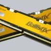
Crew Don_Dan Posted November 28, 2016 Author Crew Share Posted November 28, 2016 Interesting, I've never heard of this before. (Started with Haswell and then went backwards to 775). Thanks Don! wow thanks for making sure the info is out there I love this thread! Glad it's not lost forever You're welcome! Some of my own tests that I did two years ago. E8400 7x 572MHz, Biostar TPower I45, 2x1GB Ballistix 1:1 4-4-4-12 2T PL9 Quote Link to comment Share on other sites More sharing options...
Bullant Posted January 5, 2019 Share Posted January 5, 2019 Oh, I just bought 775 platform and this is all new to me....need to look over this and work it all out, thanks for sharing Quote Link to comment Share on other sites More sharing options...
suzuki Posted January 5, 2019 Share Posted January 5, 2019 So much info over here. Thanks for the bump Bullant. 1 Quote Link to comment Share on other sites More sharing options...
Noxinite Posted January 5, 2019 Share Posted January 5, 2019 If you have an EP45T-Extreme then you'll need this to make it actually perform reasonably in 32M. 1 1 Quote Link to comment Share on other sites More sharing options...
Bullant Posted January 5, 2019 Share Posted January 5, 2019 Yeah haven't had time to sit down and work it out, but it says can boost 25 sec in 32m....if true it's a must have. Quote Link to comment Share on other sites More sharing options...
Noxinite Posted January 5, 2019 Share Posted January 5, 2019 (edited) Well we don't have a 775 32M thread... yet. Edited January 5, 2019 by Noxinite Quote Link to comment Share on other sites More sharing options...
I.nfraR.ed Posted January 5, 2019 Share Posted January 5, 2019 (edited) I'm a 775 noob, but bought my first decent board this year and with the help of this thread I could get close to Noxinite without much work https://hwbot.org/submission/3991700_i.nfrar.ed_superpi___32m_core_2_duo_e6400_11min_39sec_110ms Should be possible to improve further. And it's interesting how much faster is DDR3. I only have Conroe chips though. < 4200MHz E6400 rankings PS: Some of the important addresses can be edited from OCX SPI Tweaker. Edited January 5, 2019 by I.nfraR.ed 1 Quote Link to comment Share on other sites More sharing options...
Bullant Posted January 5, 2019 Share Posted January 5, 2019 11 minutes ago, Noxinite said: Well we don't have a 775 32M thread... yet. Not yet we don't ? 4 minutes ago, I.nfraR.ed said: I'm a 775 noob, but bought my first decent board this year and with the help of this thread I could get close to Noxinite without much work https://hwbot.org/submission/3991700_i.nfrar.ed_superpi___32m_core_2_duo_e6400_11min_39sec_110ms Should be possible to improve further. And it's interesting how much faster is DDR3. I only have Conroe chips though. permalink noob here too, only just turned it on couple nights ago, not even a sub yet ? Quote Link to comment Share on other sites More sharing options...
Crew Antinomy Posted June 18, 2022 Crew Share Posted June 18, 2022 O.K. so I've been looking for something on my harddrive and looked through a big old archive of web pages. And found out this folder with strap tweaks from eva2000, Xavier (before) and from Coolaler forum. Xavier's posts are mentioned here but without pics are a mess to read so maybe someone will find it useful. Strap_mchbar.zip 6 Quote Link to comment Share on other sites More sharing options...
wytiwx Posted June 18, 2022 Share Posted June 18, 2022 @Antinomy Wonderful work! Thx so much! @Don_Dan Would you please re-upload your tests .jpg on TPower I45 for us? 1 Quote Link to comment Share on other sites More sharing options...
Crew Don_Dan Posted June 28, 2022 Author Crew Share Posted June 28, 2022 On 6/18/2022 at 2:36 PM, wytiwx said: Would you please re-upload your tests .jpg on TPower I45 for us? They're still online, the images are hosted on imgur, but here you go: E8400 7x 572MHz, Biostar TPower I45, 2x1GB Ballistix 1:1 4-4-4-12 2T PL9 Quote Link to comment Share on other sites More sharing options...
wytiwx Posted June 29, 2022 Share Posted June 29, 2022 (edited) Got them In my Internet, I can't see the images on imgur, the same as on some websites, so I have to turn to HWB Edited June 29, 2022 by wytiwx Quote Link to comment Share on other sites More sharing options...
Recommended Posts
Join the conversation
You can post now and register later. If you have an account, sign in now to post with your account.